
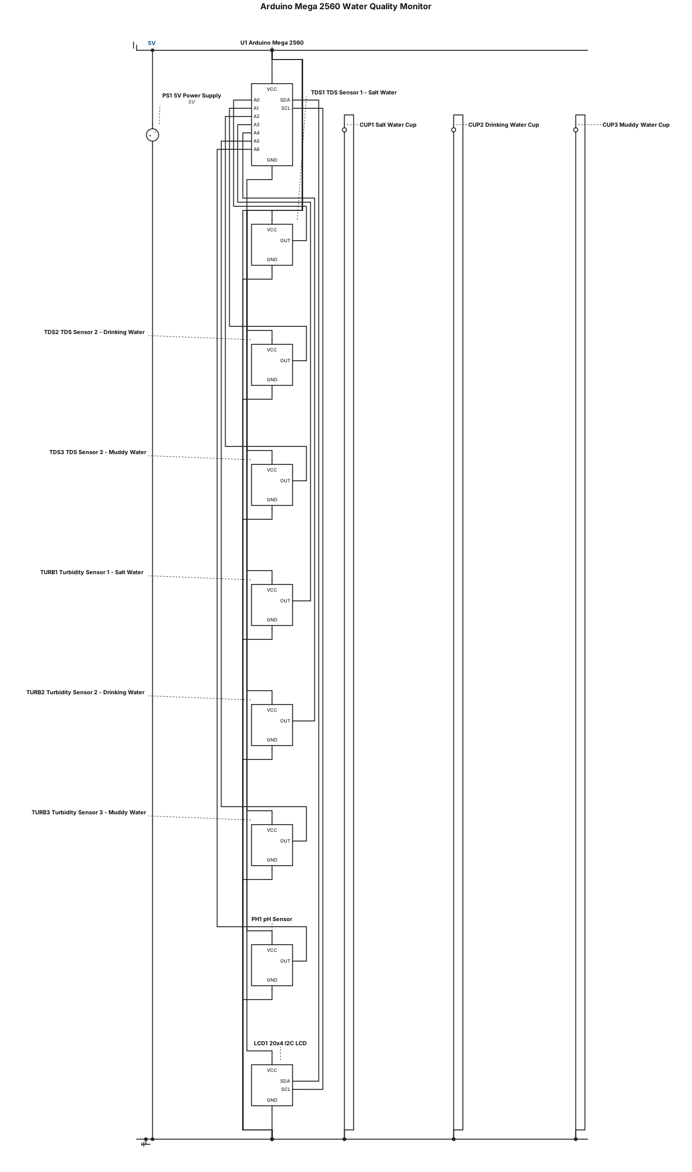
Draw a complete Arduino Mega 2560 water quality circuit with 3 TDS sensors, 3 turbidity sensors, 1 pH sensor, and a 20x4 I2C LCD. Connect all seven sensor outputs to Arduino pins A0 through A6, one sensor per pin. Connect the LCD SDA to pin 20 and SCL to pin 21. Use a 5V power supply, correct sensor voltages, and common GND for all components. Show a real breadboard with wires and 3 water cups: salt water, drinking water, and muddy water.
ENGINEERING DRAWING ARCHIVE · REAL SPECS
Engineering Diagram Examples from Real Specifications
Browse eligible circuit, ladder, single-line, P&ID, breadboard, timing, and logic drawings with their original prompts.
Browse 439 real creationsCOMMUNITY OUTPUTS · EXACT PROMPTS
All visitor creations
Showing 49–72 of 439. No stock examples or system defaults. Choose a tool, study a real result, then reopen its prompt as your starting point.
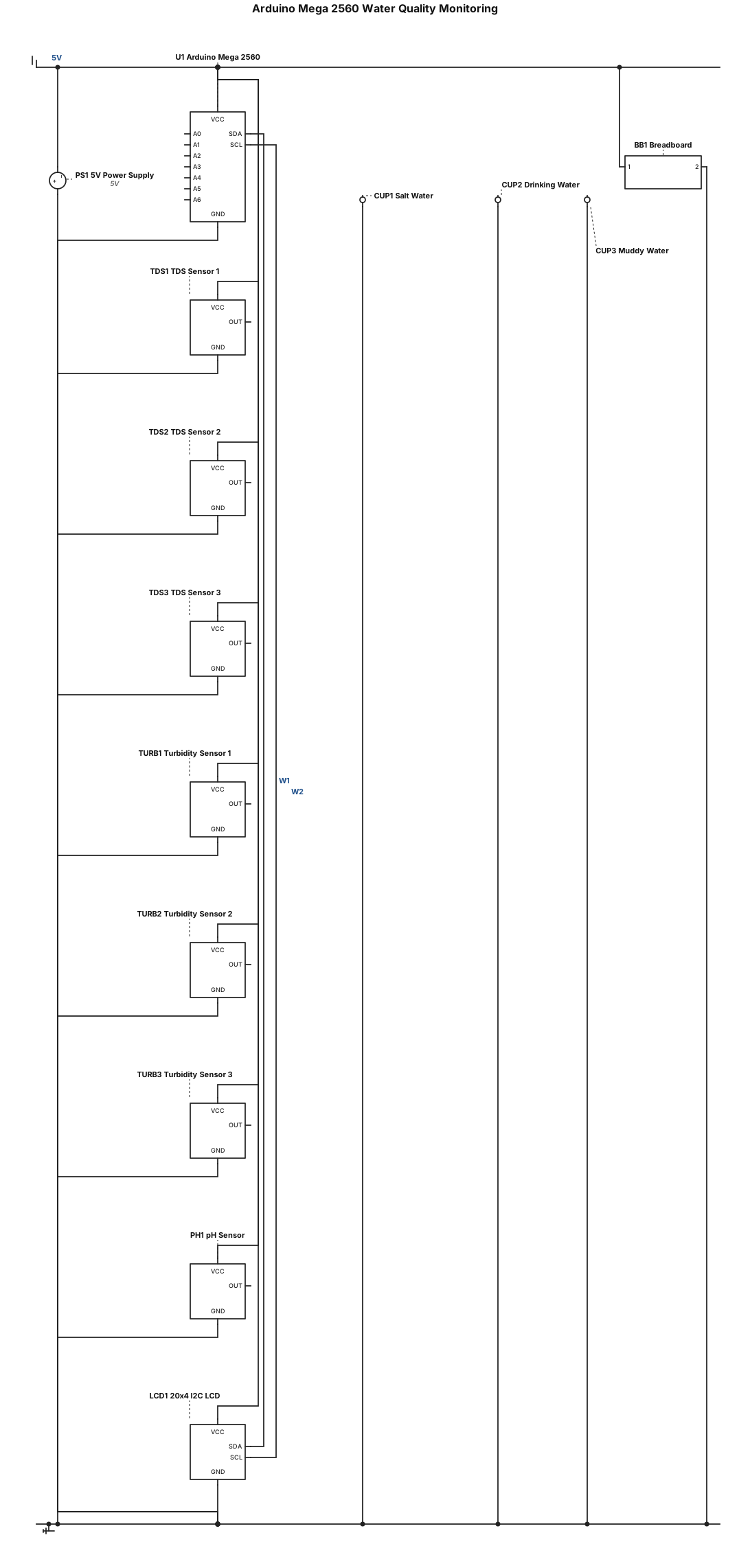
Draw a simple wiring diagram using Arduino Mega 2560, 3 TDS sensors, 3 turbidity sensors, 1 pH sensor, and a 20x4 I2C LCD. Connect the TDS sensors to A0, A1, A2, the turbidity sensors to A3, A4, A5, and the pH sensor to A6. Connect the LCD SDA to pin 20 and SCL to pin 21. Use a 5V power supply and connect all components to a common GND, using the correct voltage for each sensor. Include a breadboard and 3 water cups containing salt water, drinking water, and muddy water. Show all wires and connections clearly.
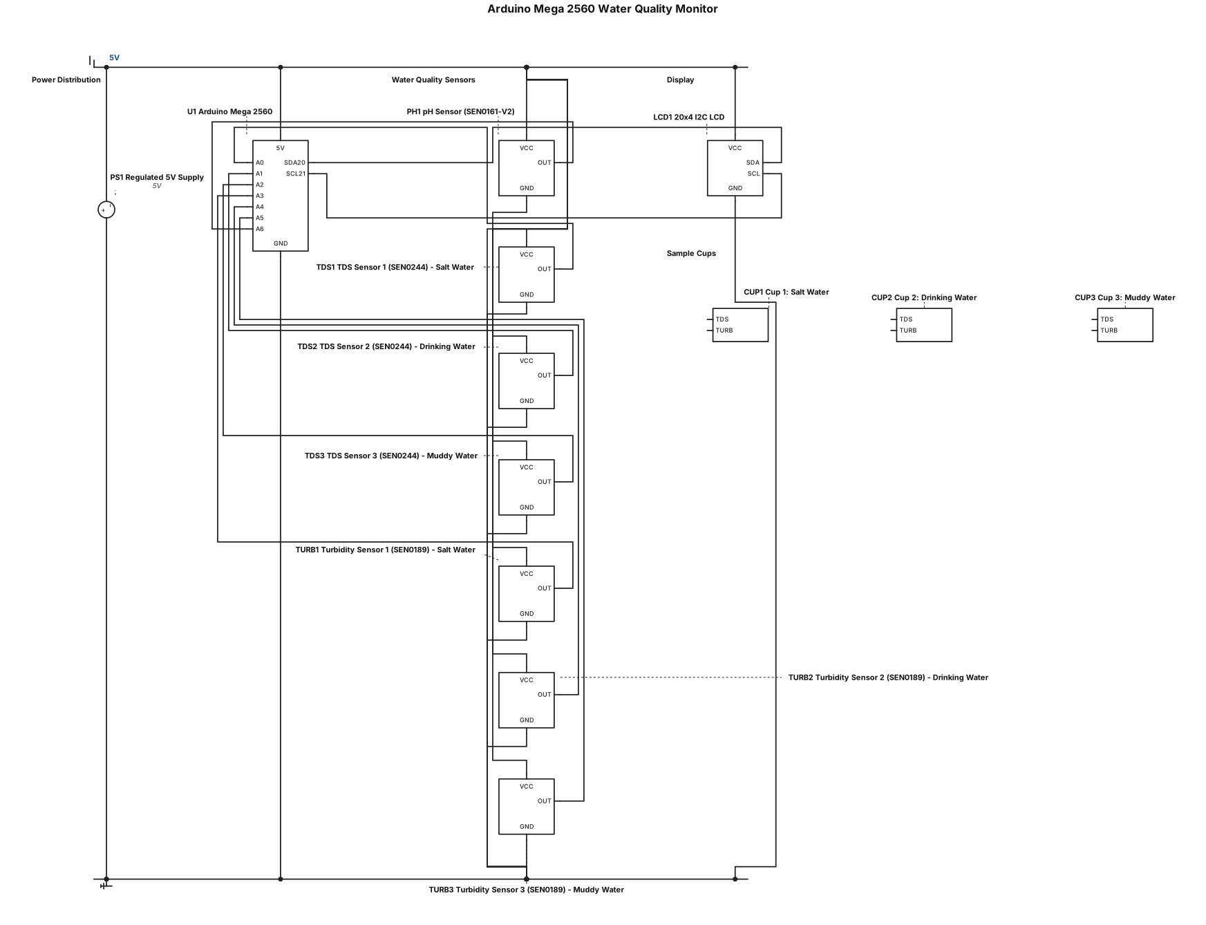
Create a realistic breadboard wiring diagram using Arduino Mega 2560, 3 TDS sensors (SEN0244), 3 turbidity sensors (SEN0189), 1 pH sensor (SEN0161-V2), and a 20x4 I2C LCD. Connect TDS sensors to A0–A2, turbidity sensors to A3–A5, pH to A6, and LCD SDA/SCL to pins 20/21. Use a regulated 5V power supply, common GND, and the correct operating voltage for each sensor module. Include 3 transparent cups containing salt water, drinking water, and muddy water, with one TDS and one turbidity sensor in each cup. Show the real breadboard, sensor modules, colored jumper wires, exact pin connections, and complete power and ground wiring.
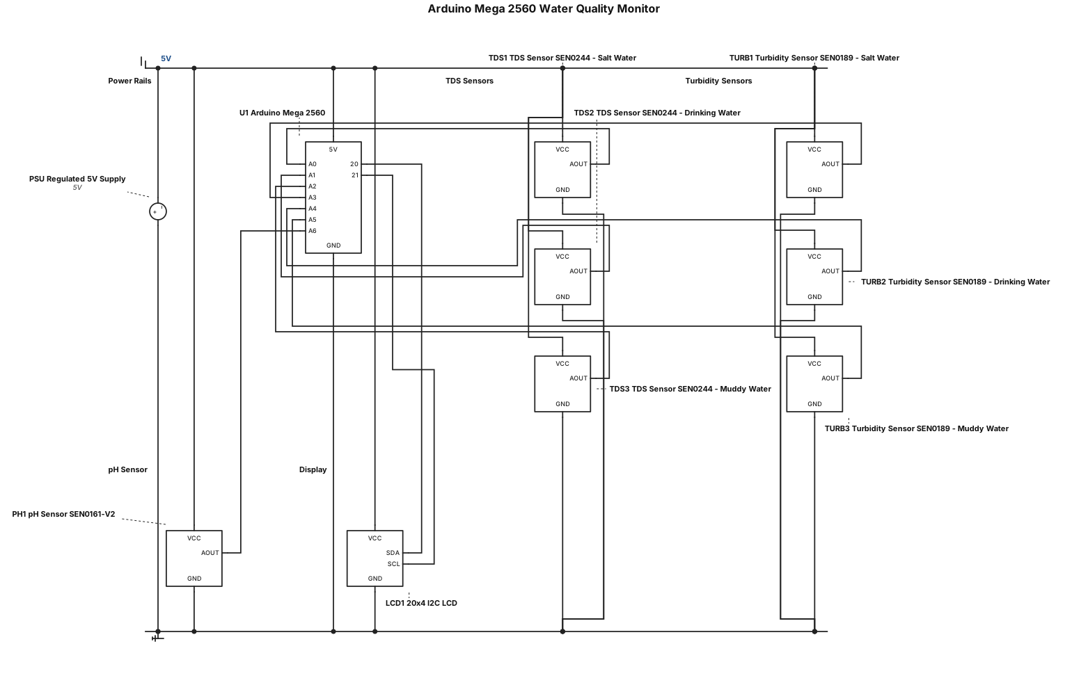
Create a realistic breadboard wiring diagram using Arduino Mega 2560, 3 TDS sensors (SEN0244), 3 turbidity sensors (SEN0189), 1 pH sensor (SEN0161-V2), and a 20x4 I2C LCD. Connect TDS sensors to A0–A2, turbidity sensors to A3–A5, pH to A6, and LCD SDA/SCL to pins 20/21. Use a regulated 5V power supply with common GND, and connect each module to its correct operating voltage. Include 3 transparent water cups: salt water, drinking water, and muddy water, with one TDS and one turbidity sensor in each cup. Show a real breadboard, all sensor modules, colored jumper wires, exact pin connections, and clearly labeled power rails. Make the circuit electrically correct and physically buildable.
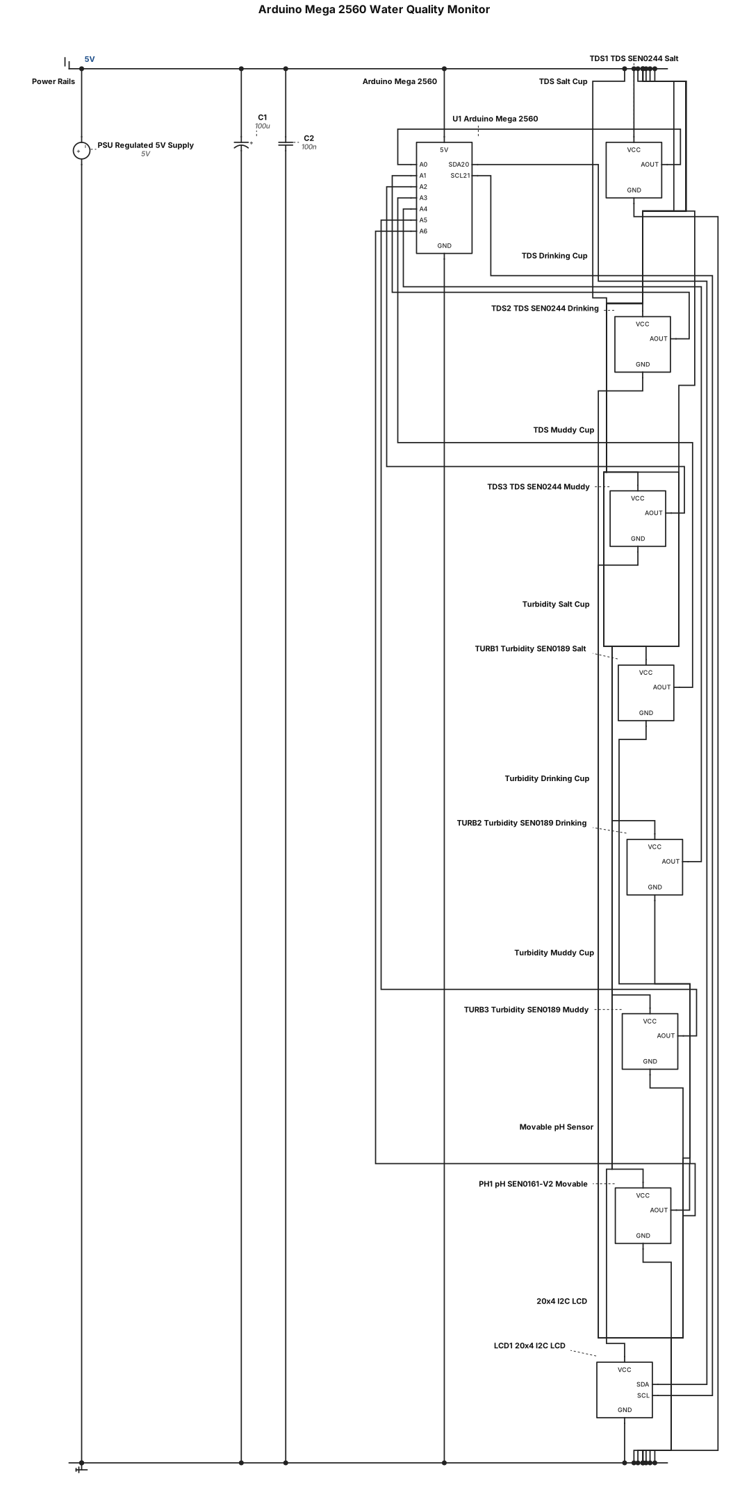
Create a realistic breadboard wiring diagram using Arduino Mega 2560, 3 TDS sensors (SEN0244), 3 turbidity sensors (SEN0189), 1 pH sensor (SEN0161-V2), and a 20x4 I2C LCD. Connect TDS sensors to A0–A2, turbidity sensors to A3–A5, pH to A6, and LCD SDA/SCL to pins 20/21. Use a regulated 5V power supply with common GND, correct sensor operating voltages, and clearly connected positive and negative breadboard rails. Include 3 water cups (salt, drinking, muddy), each with one TDS and one turbidity sensor, and one movable pH sensor. Show realistic components, sensor interface boards, all jumper wires, exact breadboard holes, and correct electrical connections.
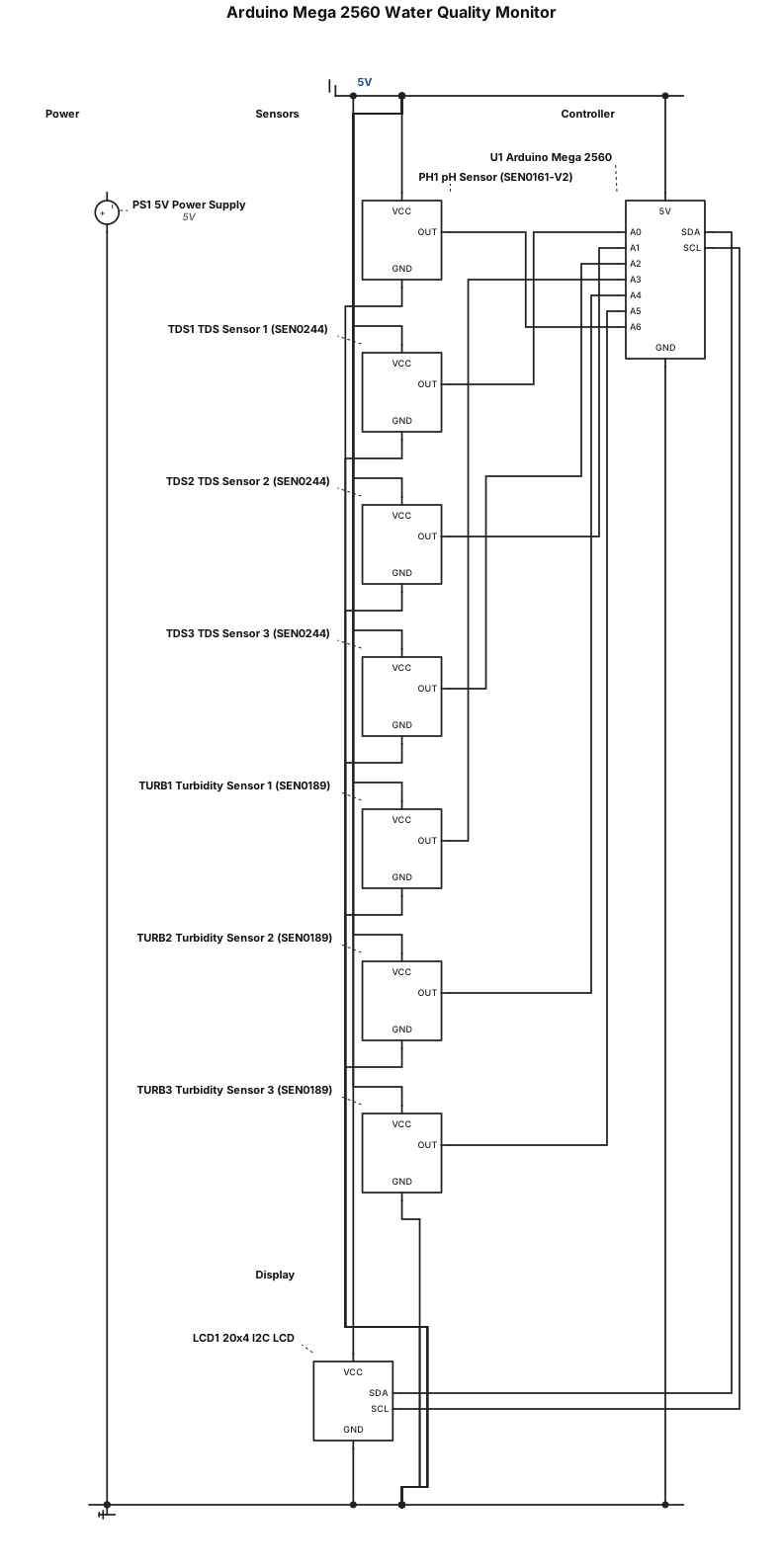
Create a complete, realistic breadboard wiring diagram using Arduino Mega 2560, 3 TDS sensors (SEN0244), 3 turbidity sensors (SEN0189), 1 pH sensor (SEN0161-V2), and a 20x4 I2C LCD. Connect TDS sensors to A0, A1, A2, turbidity sensors to A3, A4, A5, and the pH sensor to A6. Connect LCD SDA to pin 20 and SCL to pin 21. Use a suitable 5V power supply with clearly connected VCC and common GND for all compatible modules, and show every wire on a breadboard. Include 3 transparent cups: salt water, drinking water, and muddy water, each containing one TDS sensor and one turbidity sensor. The pH sensor is movable between cups. Show all real sensor modules, correct pin labels, and exact connections. Do not add unnecessary resistors or components. Make the diagram electrically accurate and ready for physical assembly.
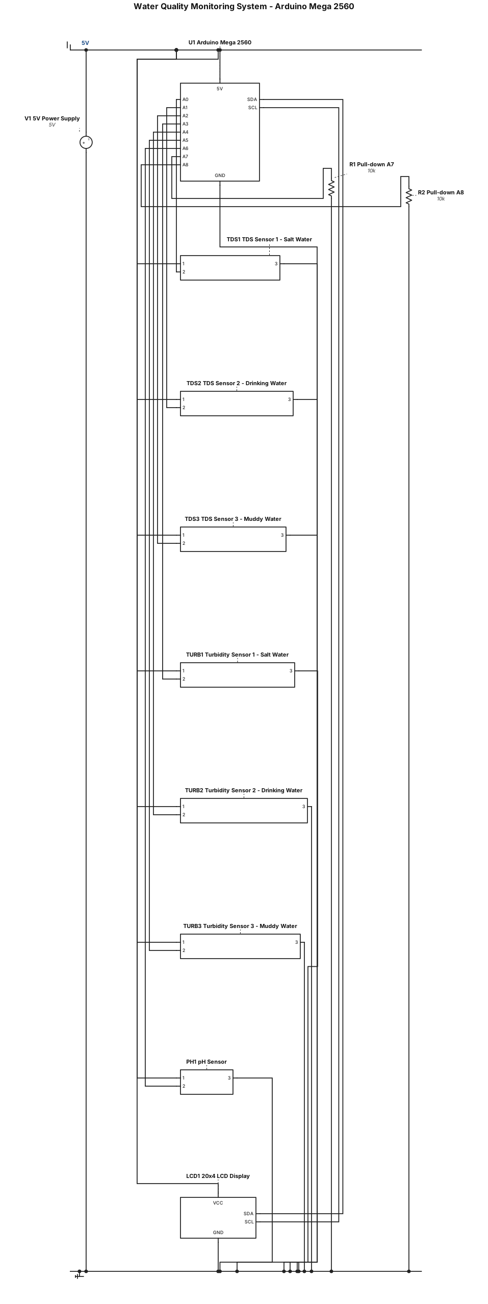
Create a complete wiring diagram for a water quality monitoring system using Arduino Mega 2560, 3 TDS sensors, 3 turbidity sensors, 1 pH sensor, and a 20x4 LCD screen. Connect all sensors and the LCD to the Arduino using a breadboard and jumper wires. The system uses a 5V power supply and has 3 water cups: salt water, drinking water, and muddy water. Please correct the wiring diagram and make sure all components are properly connected to 5V and GND. Show the positive and negative power connections, all sensor signal wires, and the Arduino Mega 2560 pin numbers. Include a breadboard and make sure the entire circuit is electrically correct and ready for real assembly.
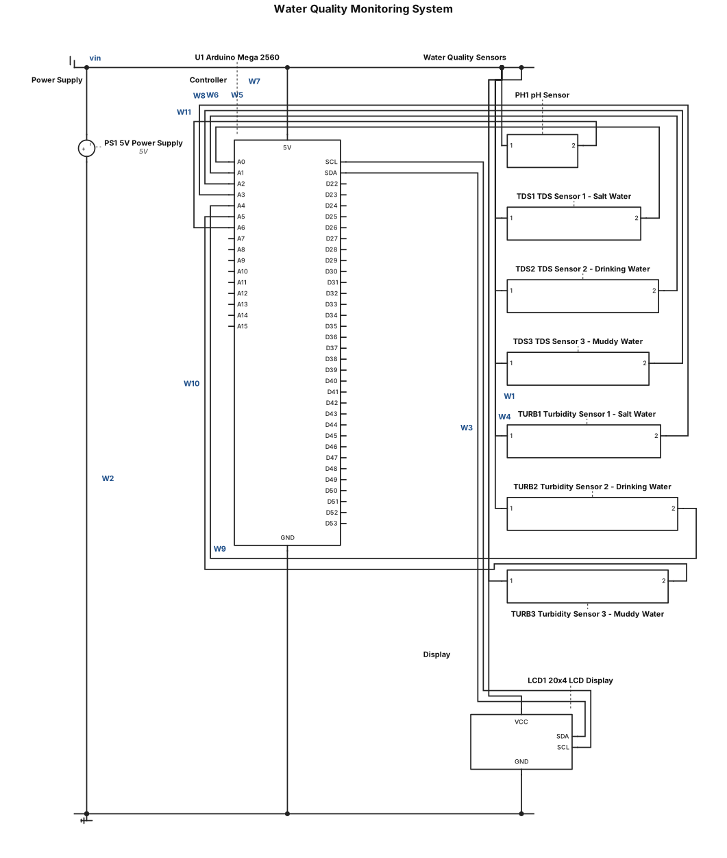
Create a complete wiring diagram for a water quality monitoring system using Arduino Mega 2560, 3 TDS sensors, 3 turbidity sensors, 1 pH sensor, and a 20x4 LCD screen. Connect all sensors and the LCD to the Arduino using a breadboard and jumper wires. The system uses a 5V power supply and has 3 water cups: salt water, drinking water, and muddy water.
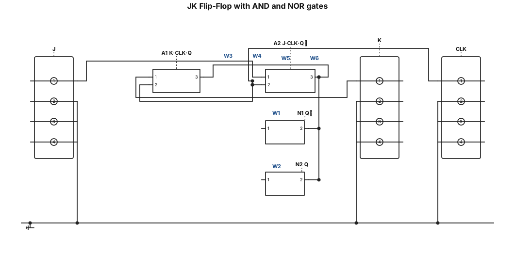
Design a JK Flip-Flop circuit exactly following this architecture: Gate arrangement: 1. Use exactly TWO AND gates in the upper section. 2. Use exactly TWO NOR gates in the lower section. 3. Arrange the two AND gates side by side at the top. 4. Arrange the two NOR gates side by side directly below the AND gates. 5. Connect the output of the left AND gate to one input of the left NOR gate. 6. Connect the output of the right AND gate to one input of the right NOR gate. Inputs and feedback: 7. Provide J, K and CLK inputs. 8. The left AND gate implements K × CLK × Q. 9. The right AND gate implements J × CLK × Q̅. 10. Connect the output Q of the right NOR gate back to the left AND gate. 11. Connect the output Q̅ of the left NOR gate back to the right AND gate. 12. Cross-couple the two NOR gates: - Left NOR output Q̅ connects to an input of the right NOR gate. - Right NOR output Q connects to an input of the left NOR gate. Outputs: 13. Left NOR output: Q̅. 14. Right NOR output: Q. Important design requirements: - Use only AND and NOR gates. - Show all self-feedback connections clearly. - Maintain the exact left-right gate arrangement described above. - Do not use NAND gates, OR gates or additional flip-flop blocks. - Generate a clean, properly labelled gate-level circuit diagram. - The circuit must implement standard JK functionality, including toggle operation when J=K=1.
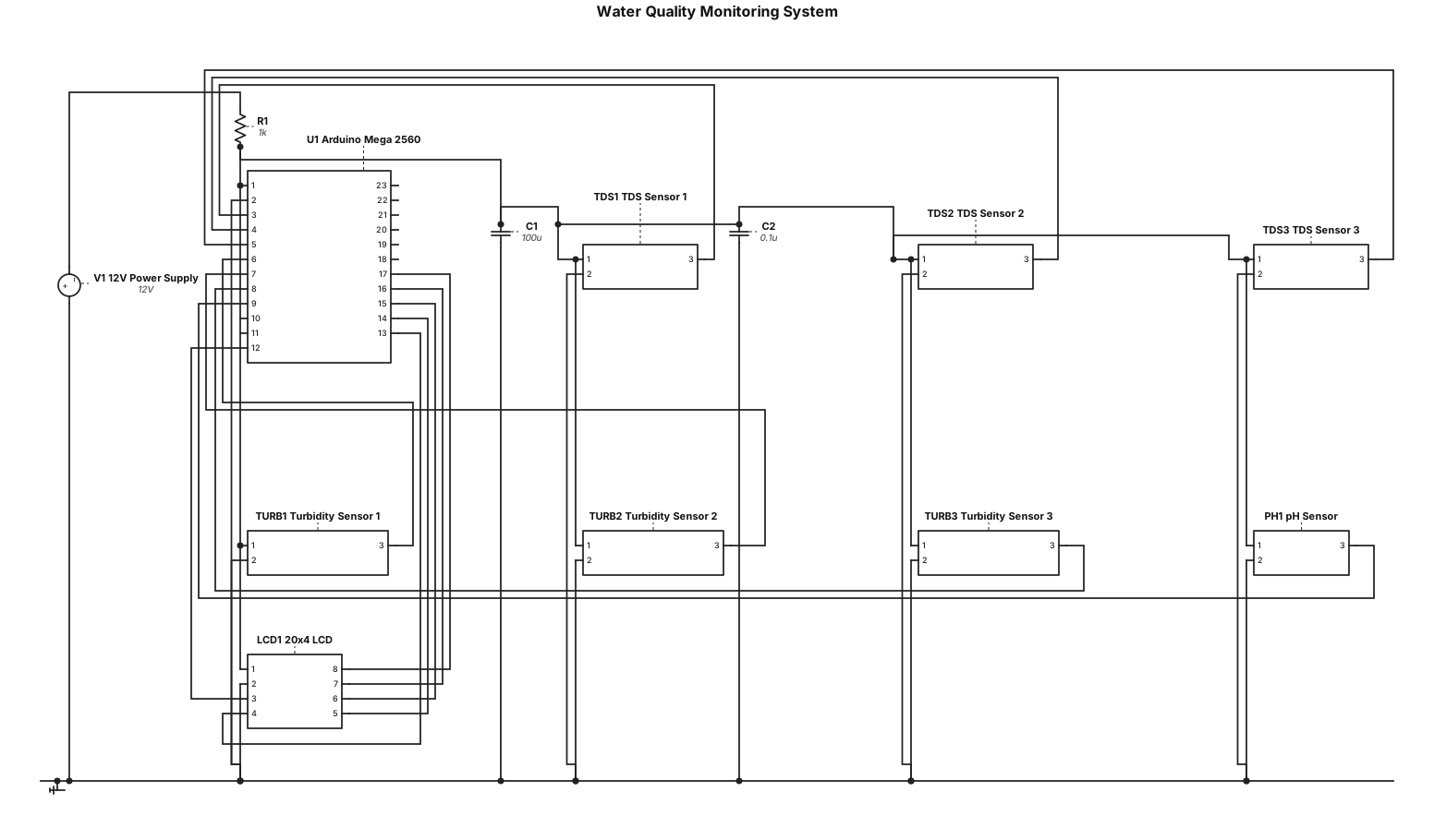
Create a complete wiring diagram for a water quality monitoring system using Arduino Mega 2560, 3 TDS sensors, 3 turbidity sensors, 1 pH sensor, and a 20x4 LCD screen.
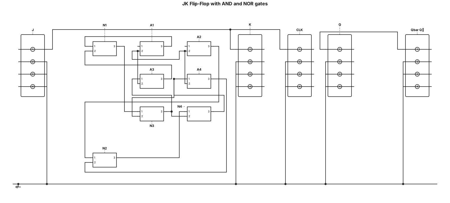
Design a JK Flip-Flop circuit using only AND gates and NOR gates with a self-feedback mechanism. Requirements: 1. Inputs: J, K and CLK (Clock). 2. Outputs: Q and Q̅ (complement of Q). 3. Use AND gates to implement the input logic. 4. Use NOR gates to construct the SR latch. 5. Implement self-feedback by connecting Q feedback to the J input logic and Q̅ feedback to the K input logic. 6. The circuit must follow the JK Flip-Flop truth table: - J=0, K=0: No change. - J=0, K=1: Reset. - J=1, K=0: Set. - J=1, K=1: Toggle. 7. Clearly label all inputs, outputs, gates and feedback connections. 8. Show the complete gate-level circuit diagram with proper wire connections. 9. Ensure that the feedback mechanism is clearly visible. In the form of flipflop ..
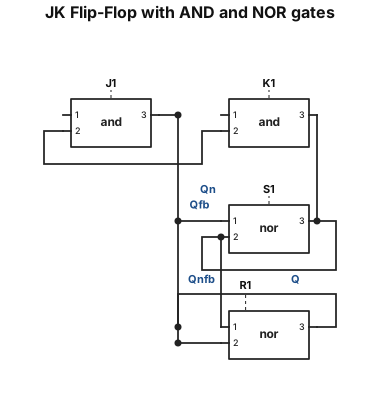
Design a JK Flip-Flop circuit using only AND gates and NOR gates with a self-feedback mechanism. Requirements: 1. Inputs: J, K and CLK (Clock). 2. Outputs: Q and Q̅ (complement of Q). 3. Use AND gates to implement the input logic. 4. Use NOR gates to construct the SR latch. 5. Implement self-feedback by connecting Q feedback to the J input logic and Q̅ feedback to the K input logic. 6. The circuit must follow the JK Flip-Flop truth table: - J=0, K=0: No change. - J=0, K=1: Reset. - J=1, K=0: Set. - J=1, K=1: Toggle. 7. Clearly label all inputs, outputs, gates and feedback connections. 8. Show the complete gate-level circuit diagram with proper wire connections. 9. Ensure that the feedback mechanism is clearly visible. In the for of flipflop ..
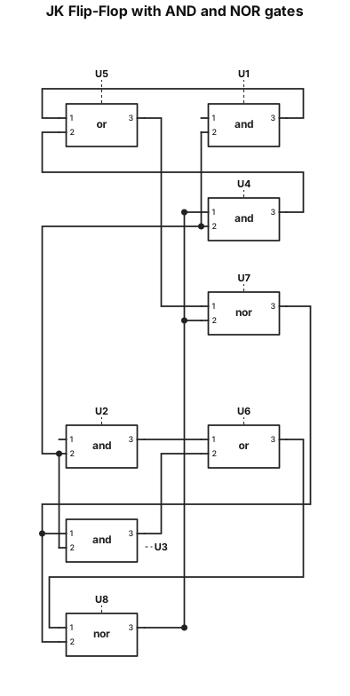
Design a JK Flip-Flop circuit using only AND gates and NOR gates with a self-feedback mechanism. Requirements: 1. Inputs: J, K and CLK (Clock). 2. Outputs: Q and Q̅ (complement of Q). 3. Use AND gates to implement the input logic. 4. Use NOR gates to construct the SR latch. 5. Implement self-feedback by connecting Q feedback to the J input logic and Q̅ feedback to the K input logic. 6. The circuit must follow the JK Flip-Flop truth table: - J=0, K=0: No change. - J=0, K=1: Reset. - J=1, K=0: Set. - J=1, K=1: Toggle. 7. Clearly label all inputs, outputs, gates and feedback connections. 8. Show the complete gate-level circuit diagram with proper wire connections. 9. Ensure that the feedback mechanism is clearly visible.
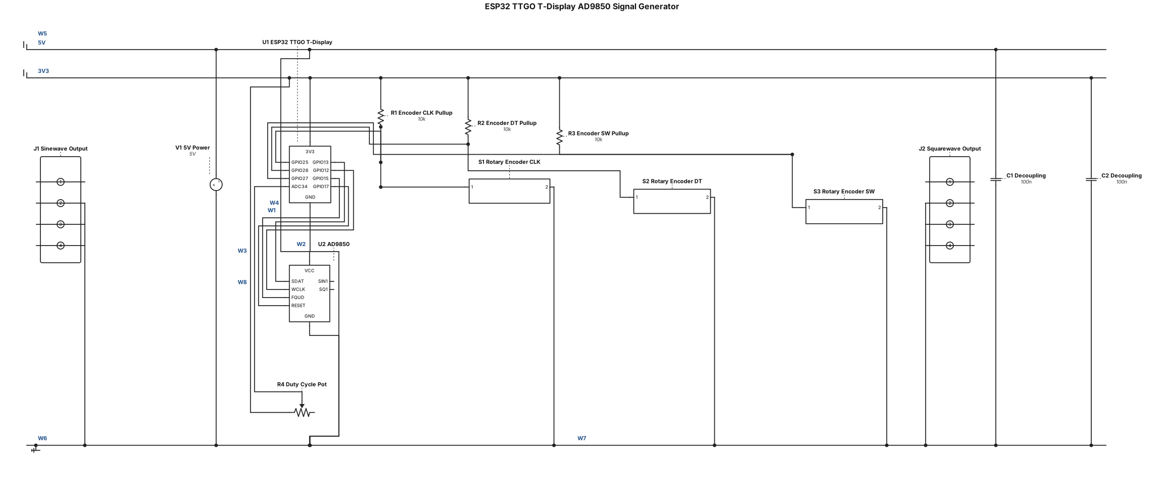
A clear technical wiring diagram and schematic blueprint, vector style, showing a complete electronics project layout with components: ESP32 TTGO T-Display microcontroller, AD9850 module, rotary encoder, potentiometer, signal output jacks, and power supply wires. The layout features clean lines and distinct labels. Connections shown: - ESP32 GPIO 13 connected to AD9850 DATA (SDAT) - ESP32 GPIO 12 connected to AD9850 W_CLK - ESP32 GPIO 15 connected to AD9850 FQ_UD - ESP32 GPIO 17 connected to AD9850 RESET - 5V power rail connected to AD9850 VCC - Common GND connection - Rotary encoder connected to ESP32 GPIO 25 (CLK), 26 (DT), 27 (SW) - Potentiometer connected for squarewave duty cycle control - Output section clearly displaying two separate simultaneous outputs: Sinewave Output from SIN1 pin, and Squarewave Output from SQ1 pin. Professional technical drawing, high contrast, white background, legible text labels, electronic schematic design.
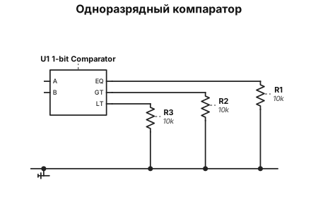
Создай три подробные цифровые логические схемы для лабораторной работы «Исследование цифровых компараторов»: 1. Одноразрядный компаратор с входами A и B и выходами A=B, A>B, A
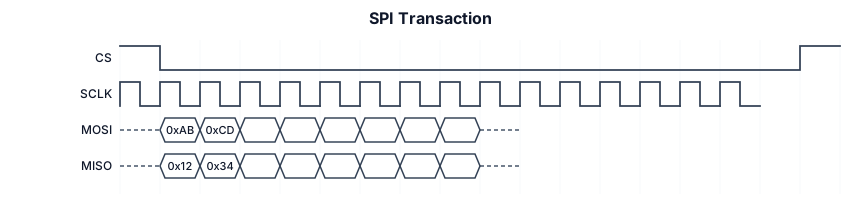
An SPI transaction timing diagram with active-low chip select, eight clock pulses, MOSI bytes 0xAB and 0xCD, and MISO bytes 0x12 and 0x34.
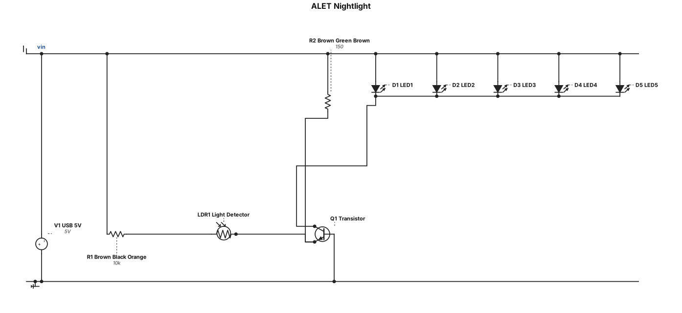
ALET nightlight that uses a USB strive kind of stick. I don’t know what it’s called like like the little attachment. You put uses 5 V. It has a light detector sensor a potential kilometre a transistor, a brown blue red resistor, a brown green brown resistor five of those and five white LEDs the transistor is one of them that looks like a D from the top like eat big cookies and yeah, that should be all you need to make a good you know all that you got
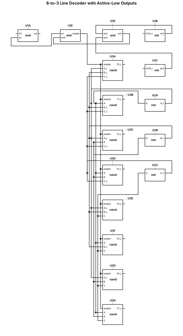
Draw a professional digital logic circuit schematic that accurately reproduces the uploaded reference image. The circuit is an 8-to-3 line decoder / 3-to-8 decoder logic diagram with active-low outputs. Requirements: Use a clean white background. Draw all logic gates using standard digital electronics symbols. On the left side, include the input signals: G1 (pin 6) G2A_L (pin 4) G2B_L (pin 5) A (pin 1) B (pin 2) C (pin 3) Include the input inverter gates and the enable logic gate exactly as shown. Draw the three input signal paths A, B, and C with their inverters and corresponding signal branches. On the right side, draw eight AND-shaped gates with small inversion bubbles at their outputs (NAND gates). Label the outputs from top to bottom: Y0_L (pin 15) Y1_L (pin 14) Y2_L (pin 13) Y3_L (pin 12) Y4_L (pin 11) Y5_L (pin 10) Y6_L (pin 9) Y7_L (pin 7) Reproduce all connecting wires, vertical signal lines, horizontal connections, junction dots, and inverter bubbles. Maintain the exact arrangement and connectivity of the reference image. Use thin black/gray lines, standard electronic symbols, and blue pin numbers. Important: Do not simplify the circuit. Do not omit any wires or connections. Do not add unnecessary components. Ensure every connection and junction matches the reference. Make the final drawing look like a precise engineering schematic, not a 3D illustration. Output: A high-resolution, clean, technically accurate circuit diagram that visually matches the uploaded reference image.
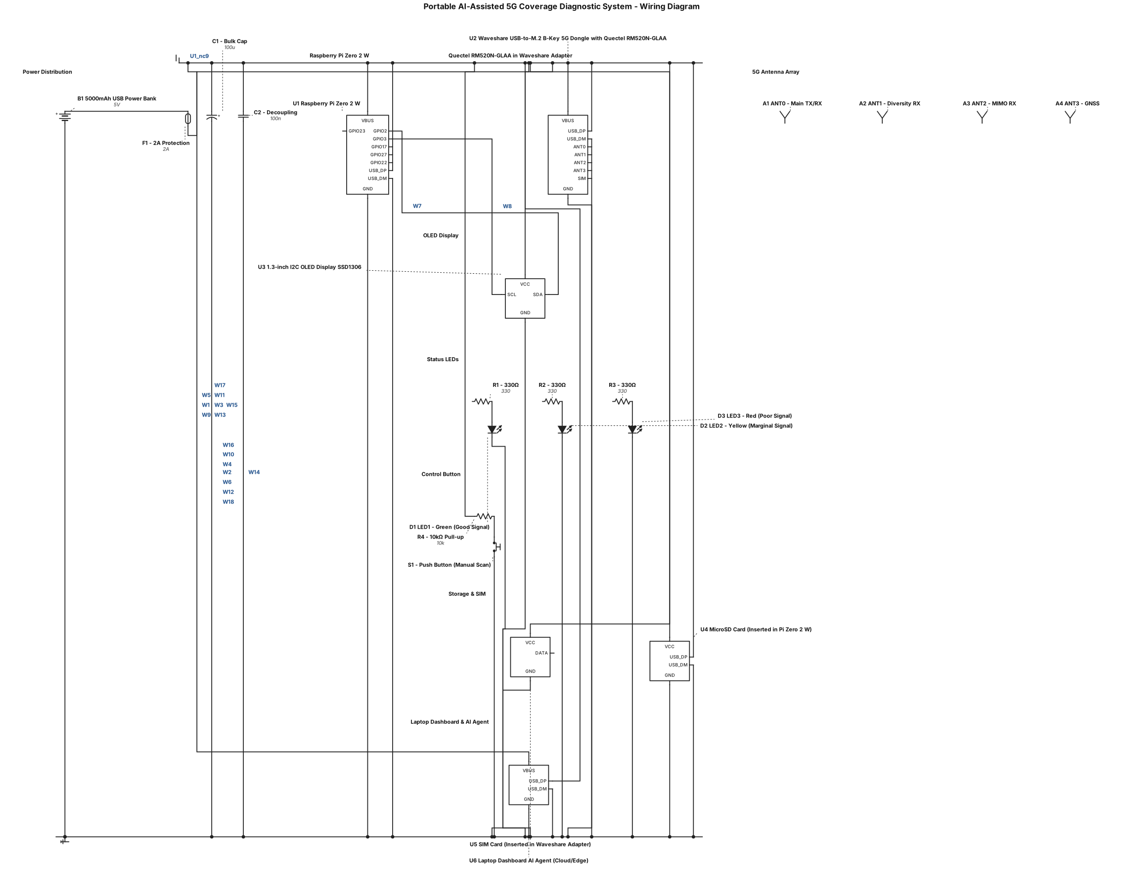
I am an electrical engineering student building a Portable AI-Assisted 5G Coverage Diagnostic System. I need a technically accurate, editable schematic and wiring diagram using these actual components: - Raspberry Pi Zero 2 W - Quectel RM520N-GLAA M.2 5G modem - Waveshare USB-to-M.2 B-Key 5G dongle with four antennas - 1.3-inch I2C OLED display - Three LEDs (green, yellow, red) with appropriate resistors - Push button - 5,000 mAh USB power bank - MicroSD card - SIM card - Laptop dashboard and AI agent The Quectel modem must remain installed inside the Waveshare adapter. Do not redraw it as a separate board or invent different hardware. Create a complete connection diagram showing the correct Raspberry Pi GPIO pin numbers, OLED I2C connections, LED resistors, button wiring, USB data connections, power distribution, and ground connections. Verify USB compatibility and modem power requirements before finalizing the diagram. If additional hardware such as a powered USB hub is required, identify it. Use exact component datasheets where available. Do not invent pinouts or connections. Clearly mark any unverified details. I need both a detailed wiring diagram for physically assembling the prototype and a clean system block diagram for my senior design presentation.
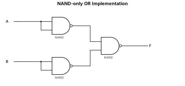
A logic gate diagram using only NAND gates to implement an OR operation, as shown in image_7.png. It features three NAND gates[cite: 3]. Inputs A and B are split: A is split and connected to both input pins of the top NAND gate (acting as an inverter for A'); B is split and connected to both input pins of the bottom-left NAND gate (acting as an inverter for B')[cite: 3]. The outputs of these two inverting NAND gates are then connected as inputs to a third, final 2-input NAND gate. Below the complete logic diagram, the text label is provided: "F=A+B=((A+B)')'=((AA)' (BB)')'" [cite: 3, 4]. All gate outlines are in the light blue color as seen in image_7.png.
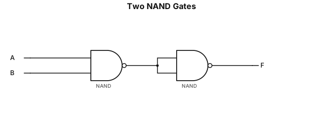
A logic gate diagram showing two NAND gates[cite: 3]. The first NAND gate has two inputs, labeled A and B. The output of the first NAND gate connects to a single dot, which then splits and connects to both input ports of the second NAND gate[cite: 3]. The final output from the second NAND gate should be labeled with the text "F=AB=((AB)')'".
A logic gate diagram showing a single NAND gate[cite: 3]. Input A splits into two branches and connects to both input pins of the NAND gate[cite: 3]. The output pin of the NAND gate is labeled as A'[cite: 3].
A logic gate diagram for F = A' using a 2-input NAND gate configured as an inverter. Input A is split into both inputs of the NAND gate, and the final output terminal is labeled as A'.
%3B%20B%20is%20split%20and%20connected%20to%20both%20input%20pins%20of%20the%20bottom-left%20NAND%20gate%20(acting%20as%20an%20inverter%20for%20B')%5Bcite%3A%203%5D.%20The%20outputs%20of%20these%20two%20inverting%20NAND%20gates%20are%20then%20connected%20as%20inputs%20to%20a%20third%2C%20final%202-input%20NAND%20gate.%20Below%20the%20complete%20logic%20diagram%2C%20the%20text%20label%20is%20provided%3A%20%22F%3DA%2BB%3D((A%2BB)')'%3D((AA)'%20(BB)')'%22%20%5Bcite%3A%203%2C%204%5D.%20All%20gate%20outlines%20are%20in%20the%20light%20blue%20color%20as%20seen%20in%20image_7.png.)
A logic gate diagram for A' using a 2-input NAND gate configured as an inverter (NOT gate). Single input A is split and connected to both inputs of the NAND gate, and the output is ( A').