
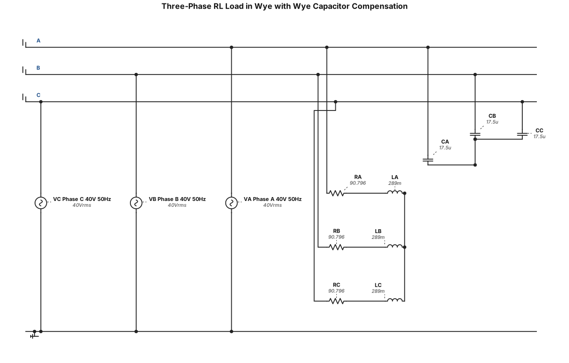
Correct the existing three-phase electrical circuit diagram for a university engineering lab report. The circuit must show **three identical RL loads connected in star (wye), with three capacitors also connected in star (wye)** for power factor correction. Use these component values: - Resistors: RA = RB = RC = 90.796 Ω - Inductors: LA = LB = LC = 289 mH - Capacitors: CA = CB = CC = 17.5 µF - Supply voltage: 40 V RMS per phase - Frequency: 50 Hz **Correct the wiring as follows:** 1. Connect phase A to resistor RA, then inductor LA, then the RL star point. 2. Connect phase B to resistor RB, then inductor LB, then the same RL star point. 3. Connect phase C to resistor RC, then inductor LC, then the same RL star point. 4. Connect capacitor CA between phase A and a separate capacitor star point. 5. Connect capacitor CB between phase B and the capacitor star point. 6. Connect capacitor CC between phase C and the capacitor star point. 7. Ensure phases A, B and C are electrically separate and no unintended connections or short circuits exist. 8. Show a balanced three-phase AC supply with 120-degree phase separation. Use standard electrical schematic symbols, black lines on a white background, and clearly label all components. **Important:** Each RL branch must connect to a different phase. The capacitors must form a proper star connection, not delta. The diagram should be technically correct, neat and suitable for an ELEC2132 laboratory report. Title: Three-Phase RL Load in Wye with Wye Capacitor Compensation.
Engineering Diagram Examples from Real Specifications
Browse eligible circuit, ladder, single-line, P&ID, breadboard, timing, and logic drawings with their original prompts.
Browse 538 real creationsSchematic
Showing 1–24 of 35. No stock examples or system defaults. Choose a tool, study a real result, then reopen its prompt as your starting point.
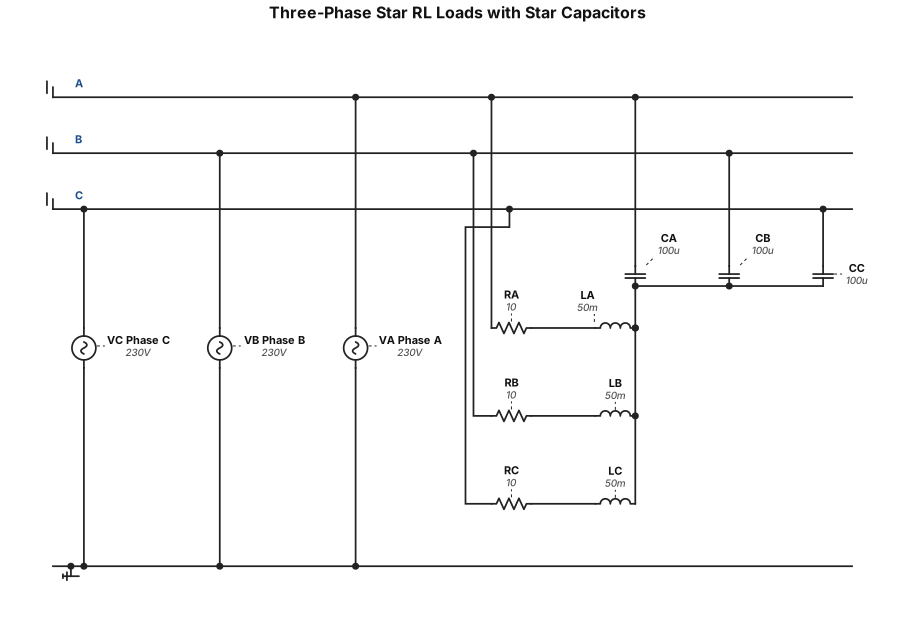
Draw a three-phase electrical circuit with three identical RL loads connected in a star (wye) configuration. Each load consists of a resistor and inductor connected in series. Add three capacitors connected in star (wye) across the three-phase supply. Label the supply lines A, B and C. Use standard electrical symbols and a clean black-and-white schematic.
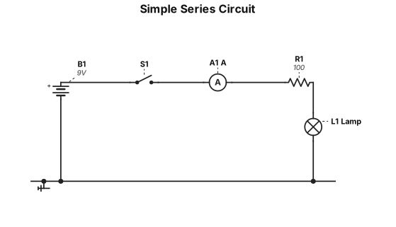
"Create a simple electrical circuit diagram for a school science assignment. Include a battery, a light bulb, a switch, an ammeter, and a resistor. Connect all five components in one complete series circuit using standard electrical symbols. Make sure the ammeter is connected in series and the switch controls the light bulb."
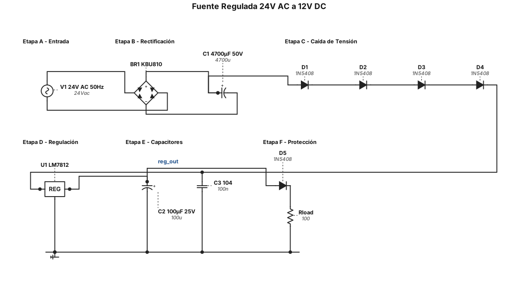
Diseña un circuito electrónico interactivo y simúlalo. Quiero una interfaz visual moderna, atractiva, intuitiva y profesional, similar a un laboratorio virtual de electrónica. **PROYECTO: FUENTE REGULADA 24 V AC → 12 V DC** ### 1. DISEÑO VISUAL - Fondo claro, cuadrícula electrónica tenue. - Componentes electrónicos realistas y reconocibles. - Cables positivos en rojo y masa en negro. - Entrada AC en azul. - Componentes distribuidos horizontalmente, de izquierda a derecha. - Terminales y patas claramente separados. - Etiquetas pequeñas, legibles y sin superposiciones. - Valores de tensión visibles junto a cada etapa. - Instrumentos virtuales para medir voltaje y corriente. - Panel inferior con osciloscopio y gráficos de tensión. ### 2. CIRCUITO Construir las siguientes etapas: **ETAPA A — ENTRADA** - Fuente de 24 V AC RMS. - Frecuencia de 50 Hz. - Dos terminales de entrada. **ETAPA B — RECTIFICACIÓN** - Puente rectificador KBU810. - Capacitor C1 de 4700 µF / 50 V. - Positivo y negativo correctamente conectados. - Mostrar la tensión continua rectificada. **ETAPA C — CAÍDA DE TENSIÓN** - Cuatro diodos 1N5408 conectados en serie. - Orientación directa: ánodo hacia la entrada positiva y cátodo hacia la salida. - Mostrar la caída total de tensión. **ETAPA D — REGULACIÓN** Utilizar un LM7812 real o su modelo SPICE. Representar el componente en vista frontal, con tres patas físicas independientes: - PATA 1 IZQUIERDA: INPUT. - PATA 2 CENTRAL: GND. - PATA 3 DERECHA: OUTPUT. No superponer, unir ni intercambiar las patas. **ETAPA E — CAPACITORES** - C3: 100 nF, código 104. Una pata exclusivamente al pin 1. La otra pata exclusivamente al pin 2 (GND). - C2: 100 µF / 25 V. Positivo al pin 3. Negativo al pin 2 (GND). Ambos capacitores deben tener sus dos terminales visibles y conexiones independientes. **ETAPA F — PROTECCIÓN** - D
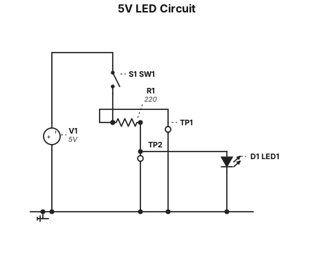
A 5 V LED circuit with a 220 ohm series resistor, an SPST switch, and labeled test points before and after the resistor.
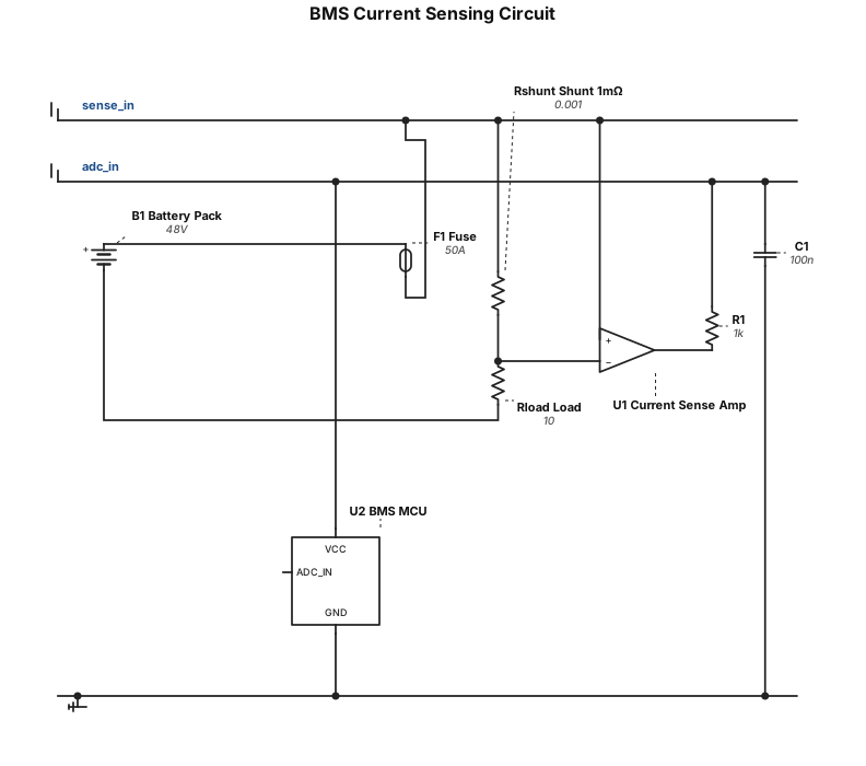
bms current sensing circuit
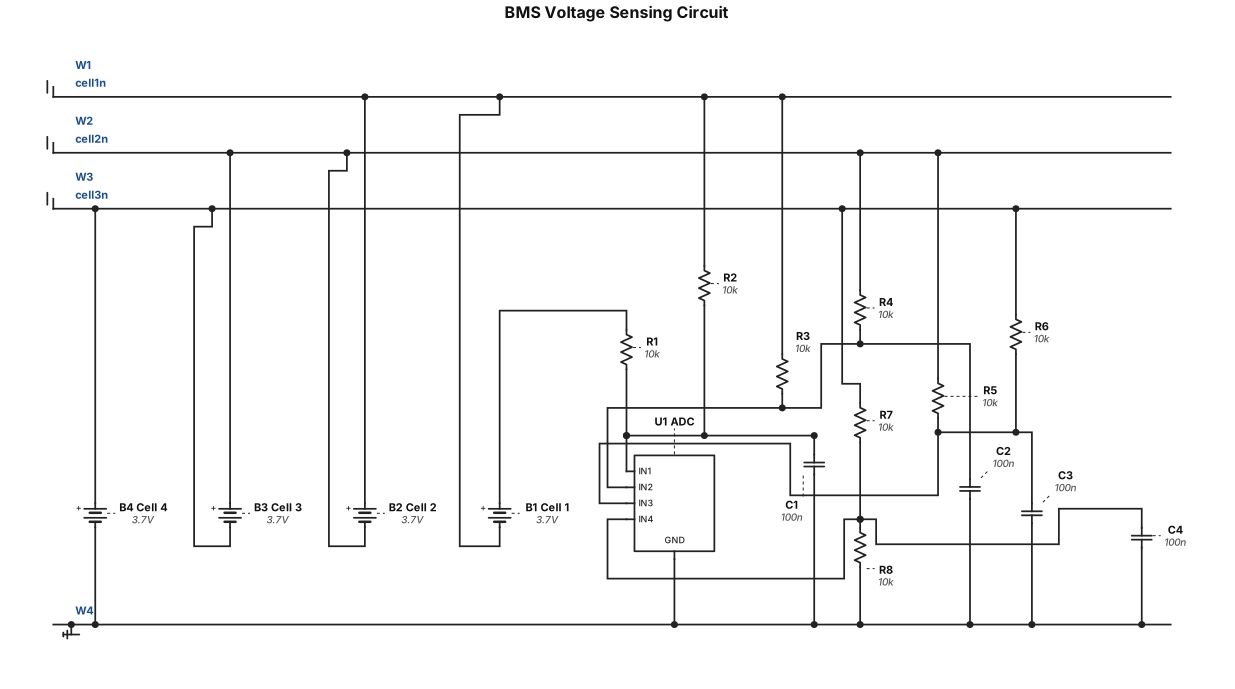
bms voltage sensing circuit
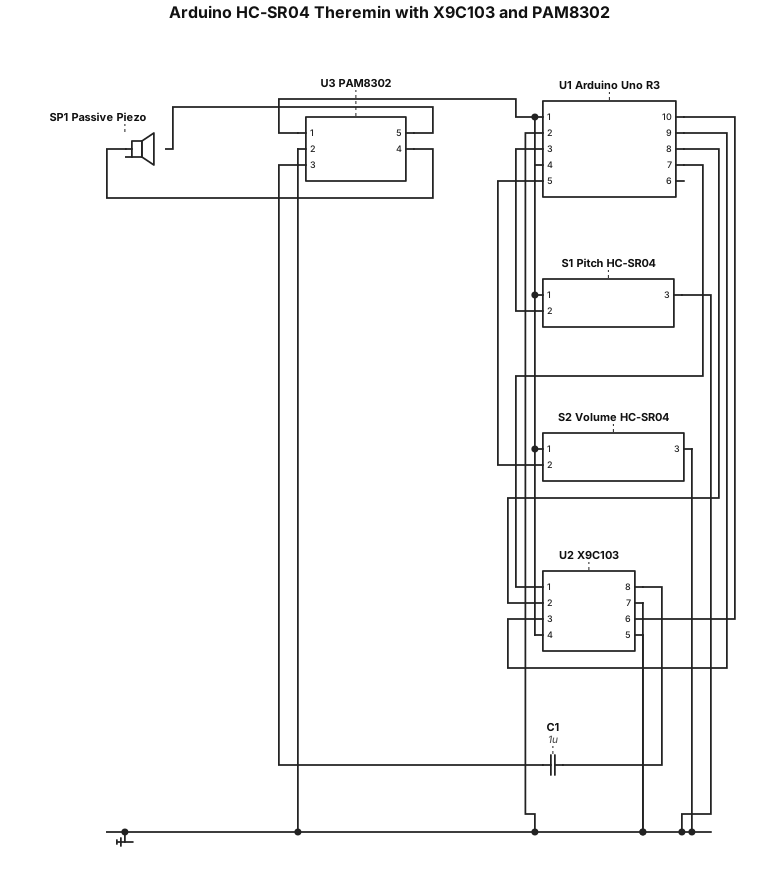
This uses an arduino uno r3 and two HC-SR04 sensors: one controls pitch and one controls volume. The X9C103 attenuates the Arduino’s tone signal before it reaches the PAM8302; the PAM8302 drives the passive piezo. Connections Pitch HC-SR04: TRIG → D2, ECHO → D3 Volume HC-SR04: TRIG → D4, ECHO → D5 Arduino D9 (tone signal) X9C103 RH X9C103 RL → GND; RW → PAM8302 audio input X9C103 CS → D6, INC → D7, U/D → D8; VCC → 5V, VSS → GND PAM8302 power and input ground common GND Passive piezo PAM8302 OUT+ and OUT− Use the PAM8302 breakout’s audio input. If it has no input coupling capacitor, add a 1 µF capacitor in series between RW and the amplifier input. Do not connect either PAM8302 speaker output to GND; its outputs are bridge-tied. Check your breakout’s supply-voltage rating.
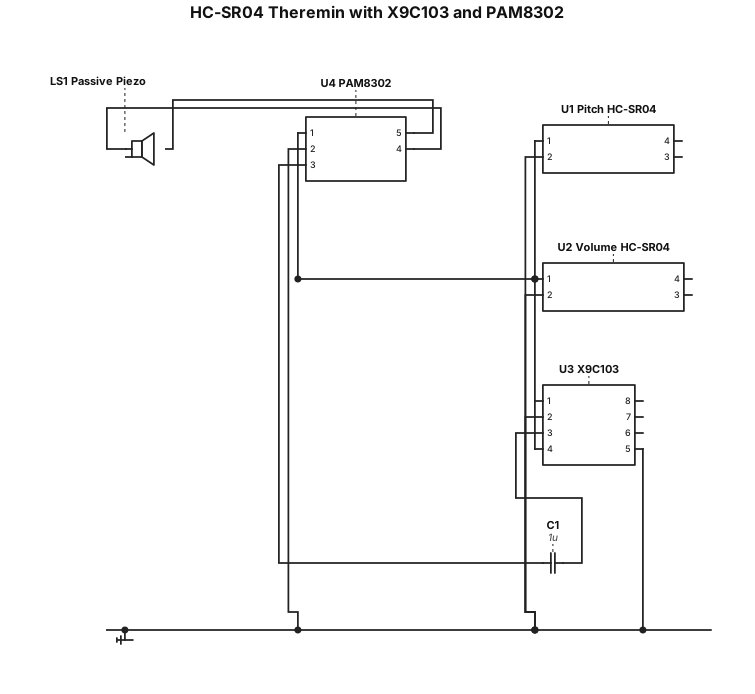
This uses two HC-SR04 sensors: one controls pitch and one controls volume. The X9C103 attenuates the Arduino’s tone signal before it reaches the PAM8302; the PAM8302 drives the passive piezo. Connections Pitch HC-SR04: TRIG → D2, ECHO → D3 Volume HC-SR04: TRIG → D4, ECHO → D5 Arduino D9 (tone signal) X9C103 RH X9C103 RL → GND; RW → PAM8302 audio input X9C103 CS → D6, INC → D7, U/D → D8; VCC → 5V, VSS → GND PAM8302 power and input ground common GND Passive piezo PAM8302 OUT+ and OUT− Use the PAM8302 breakout’s audio input. If it has no input coupling capacitor, add a 1 µF capacitor in series between RW and the amplifier input. Do not connect either PAM8302 speaker output to GND; its outputs are bridge-tied. Check your breakout’s supply-voltage rating.
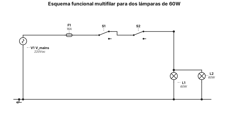
hazme un esquema funcional multifilar para accionar dos laparas de 60w si se funde una la oitra no funciona desde dos interruptores q cuplan la tabla d ela verdsd
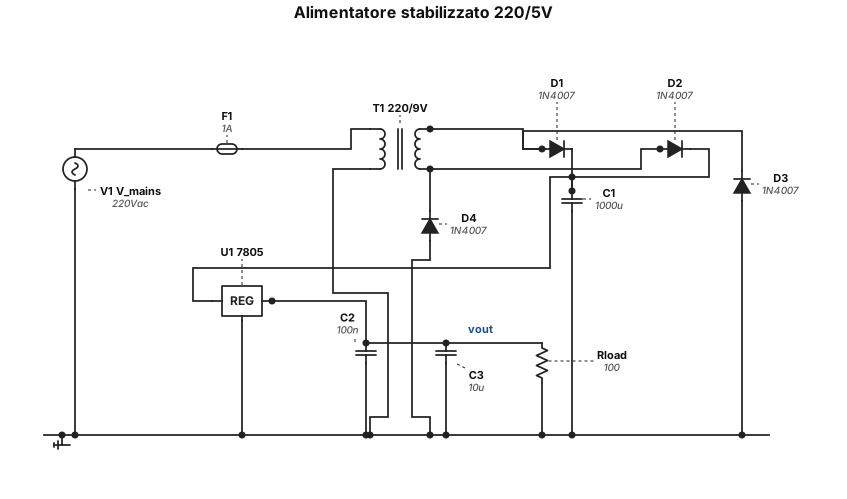
alimentatore stabilizzato 220/5 V
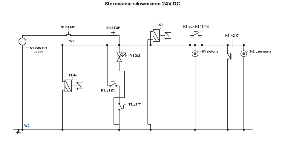
Narysuj profesjonalny, czytelny schemat elektryczny w standardzie przemysłowym IEC, w formie drabinkowej LADDER. Elementy układu: - S1 — przycisk START NO - S0 — przycisk STOP NC - K1 — przekaźnik z podtrzymaniem przez styk pomocniczy NO 13-14 - T1 — przekaźnik czasowy ustawiony na 4 sekundy - Y1 — cewka elektrozaworu 3/2 z powrotem sprężynowym - H1 — lampka sygnalizacyjna zielona - H2 — lampka sygnalizacyjna czerwona - Zasilanie sterowania 24 V DC Zasada działania: 1. Po krótkim naciśnięciu START układ uruchamia się i przekaźnik K1 podtrzymuje się. 2. Elektrozawór Y1 włącza się i siłownik jednostronnego działania wysuwa się. 3. Podczas wysuwania świeci zielona lampka H1, a czerwona H2 jest wyłączona. 4. Po 4 sekundach układ wyłącza Y1. Zawór wraca sprężyną i siłownik chowa się. 5. Gdy siłownik jest w pozycji spoczynkowej, zielona lampka H1 jest wyłączona, a czerwona H2 świeci. 6. Przycisk STOP wyłącza układ. Wykonaj osobne linie drabinkowe dla przekaźnika, podtrzymania, czasówki, elektrozaworu oraz obu lampek. Zieloną lampkę podłącz tak, aby świeciła podczas zasilania cewki Y1. Czerwoną lampkę podłącz przez odpowiedni styk przekaźnika, aby świeciła w stanie spoczynkowym, a gasła podczas wysuwania. Zastosuj symbole IEC, numery styków, oznaczenia przewodów i czytelne opisy. Uporządkuj schemat symetrycznie, bez krzyżujących się przewodów. Nie twórz schematu blokowego. Sprawdź poprawność logiczną układu.
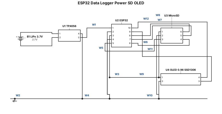
1. Power & Charging Subsystem (TP4056 & Battery)3.7V LiPo Battery Positive (+) $\rightarrow$ TP4056 B+ pad3.7V LiPo Battery Negative (-) $\rightarrow$ TP4056 B- padTP4056 OUT+ (Power Output) $\rightarrow$ ESP32 VIN (or 5V) pinTP4056 OUT- (Ground Output) $\rightarrow$ ESP32 GND pinNote: Recharging is handled via the onboard Type-C port on the TP4056 module.2. MicroSD Card Module (SPI Interface)VCC $\rightarrow$ ESP32 3V3 pinGND $\rightarrow$ ESP32 GND pinCS (Chip Select) $\rightarrow$ ESP32 GPIO 5 (labeled D5)SCK (Serial Clock) $\rightarrow$ ESP32 GPIO 18 (labeled D18)MISO (Master In Slave Out) $\rightarrow$ ESP32 GPIO 19 (labeled D19)MOSI (Master Out Slave In) $\rightarrow$ ESP32 GPIO 23 (labeled D23)3. OLED Display (0.96" SSD1306, I2C Interface)VCC $\rightarrow$ ESP32 3V3 pinGND $\rightarrow$ ESP32 GND pinSCL (Serial Clock) $\rightarrow$ ESP32 GPIO 22SDA (Serial Data) $\rightarrow$ ESP32 GPIO 21
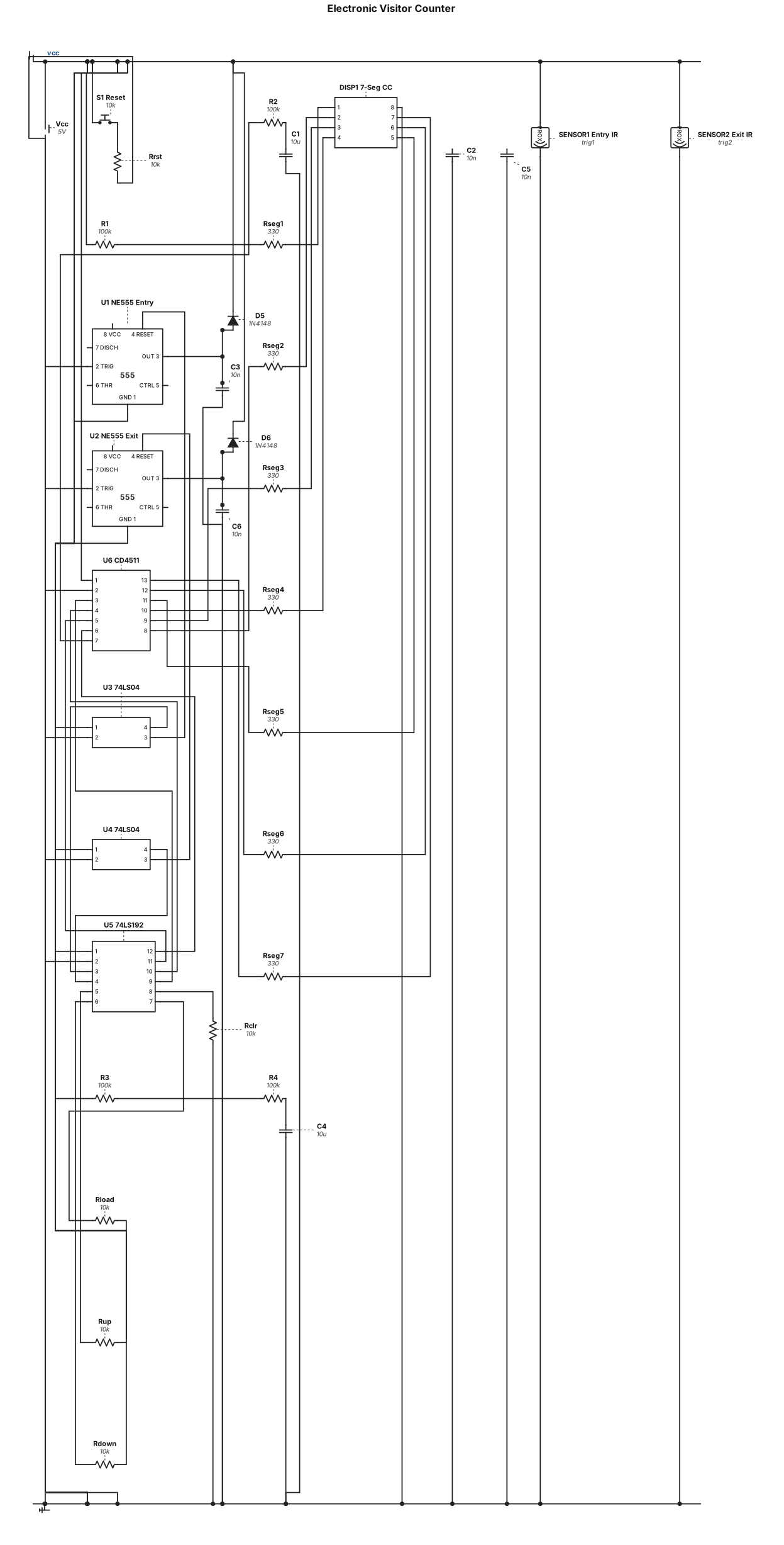
Draw a detailed electronic schematic for a microcontroller-free Electronic Visitor Counter. Components: - Two digital-output IR sensor modules: entry and exit. - Two NE555 ICs configured as monostable pulse conditioners. - One 7404/74LS04 inverter IC. - One 74LS192 BCD up/down counter. - One CD4511 BCD-to-7-segment decoder. - One common-cathode 7-segment display. - Timing resistors and capacitors, current-limiting resistors, a reset push button, and a regulated 5 V supply. Operation: 1. Entry sensor generates one count-up event. 2. Exit sensor generates one count-down event. 3. NE555 circuits condition the sensor signals. 4. The inverter stages provide the required signal polarity. 5. The 74LS192 counts up or down. 6. Its four BCD outputs drive the CD4511. 7. The CD4511 drives the common-cathode display through individual segment resistors. Draw the actual IC symbols with pin numbers. Show every power, ground, clock, reset, timing, and display connection. Label all components and values. Use clear wires and junction dots. Verify the IC pinouts and clock polarities against the datasheets. Do not invent connections. Identify any incompatible components or missing logic. The NE555 monostable must not be assumed to prevent repeated counts during sustained sensor activation. Include appropriate retrigger-prevention logic. Generate a clean, readable circuit schematic rather than a block diagram. If the full circuit is too complex, generate separate schematics for the sensor/timer stages, counter, and display.
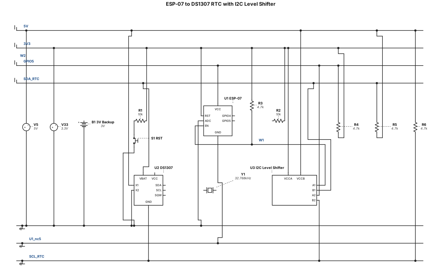
Create an accurate electrical schematic connecting an ESP-07 ESP8266MOD 16-pin module to a DS1307 RTC DIP-8 IC. ESP-07 connections: - Pin 1 RST: connect a normally-open pushbutton from RST to GND, plus a separate 10kΩ pull-up resistor from RST to 3.3V. - Pin 2 ADC: NC, no connection. - Pin 3 EN/CH_PD: separate 10kΩ pull-up resistor to 3.3V. - Pin 8 VCC: regulated 3.3V. - Pin 9 GND: common ground. - Pin 13 GPIO4: I2C SDA. - Pin 14 GPIO5: I2C SCL. DS1307 DIP-8 pinout, top view with notch at the top: 1 X1, 2 X2, 3 VBAT, 4 GND, 5 SDA, 6 SCL, 7 SQW/OUT, 8 VCC. DS1307 connections: - Pins 1 and 2: connect a 32.768kHz crystal between X1 and X2. - Pin 3 VBAT: positive of a 3V backup battery; battery negative to common ground. - Pin 4 GND: common ground. - Pin 5 SDA: connect to ESP GPIO4 through a bidirectional I2C level shifter. - Pin 6 SCL: connect to ESP GPIO5 through the same level shifter. - Pin 7 SQW/OUT: NC. - Pin 8 VCC: regulated 5V. Include a correctly wired bidirectional I2C level shifter, with 3.3V pull-ups on the ESP side and 5V pull-ups on the DS1307 side. Never apply 5V to any ESP8266 GPIO. Draw a clean black-and-white engineering schematic with exact pin numbers, straight wires, visible junction dots, separate 3.3V and 5V rails, and common ground. Do not invent or swap pin connections. If a connection cannot be drawn reliably, label it for verification instead of guessing.
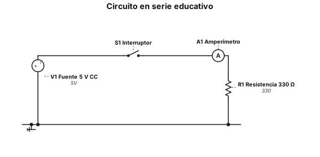
Crea un esquema eléctrico educativo, muy sencillo y claramente etiquetado, de un circuito en serie con una fuente de corriente continua de 5 V, un interruptor y una resistencia de 330 Ω. Muestra todos los cables, los terminales positivo y negativo, y un amperímetro conectado en serie. Fondo blanco, líneas claras y etiquetas grandes en español. No agregues componentes adicionales.
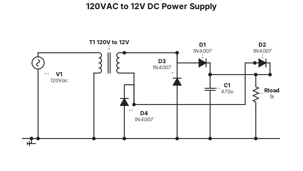
A tranformer to step down 120VAC power to 12V and a full wave bridge rectifier to rectify AC
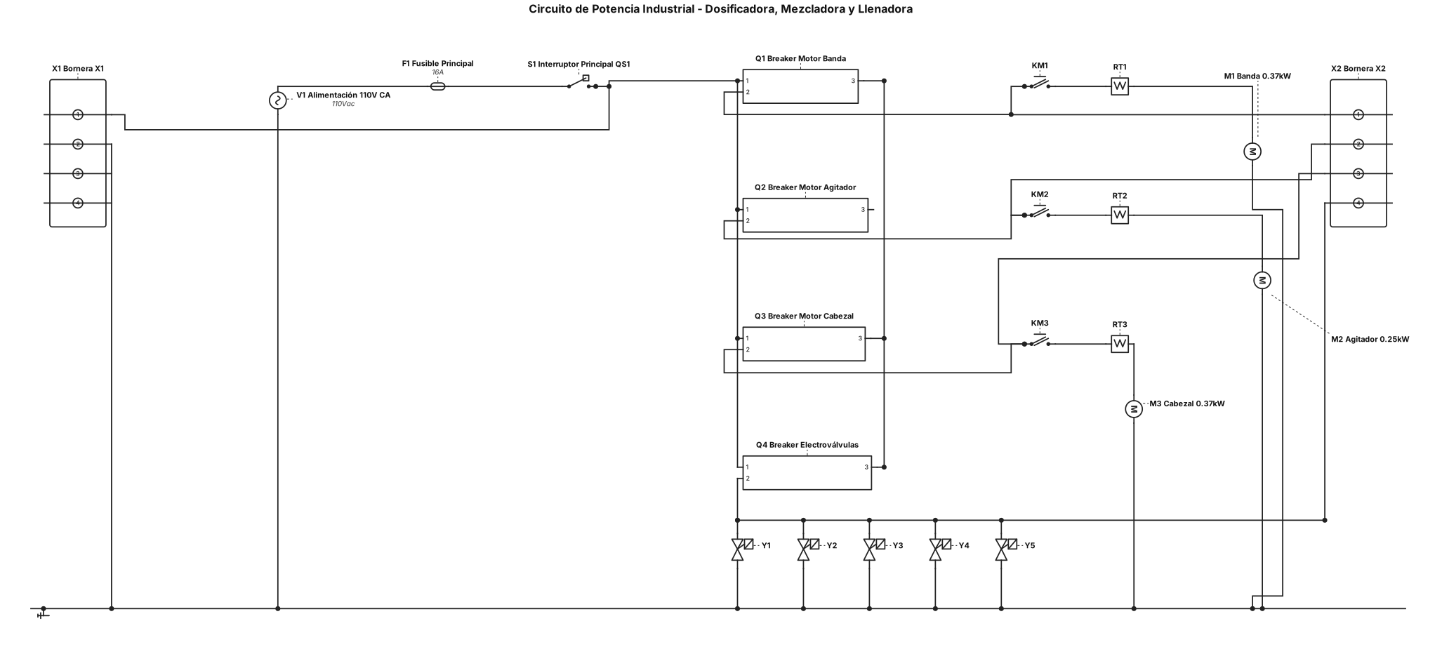
Diseña el circuito de potencia industrial de una máquina automática dosificadora, mezcladora y llenadora. Alimentación 110 V CA. Incluir interruptor principal, breakers, contactores KM1, KM2 y KM3, relés térmicos RT1, RT2 y RT3, motor M1 de banda 0,37 kW, motor M2 agitador 0,25 kW y motor M3 de cabezal 0,37 kW. Incluir electroválvulas Y1 a Y5 de 110 V CA y borneras. Utilizar simbología IEC y mostrar claramente las conexiones de potencia
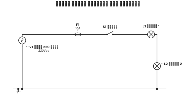
دائرة لتشغيل مصباحين على التوالي
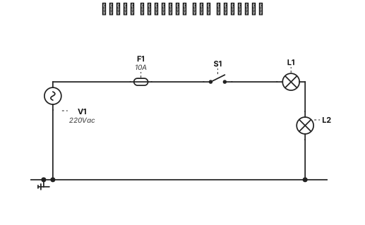
دائرة ل تشغيل مصباحين على التوالي
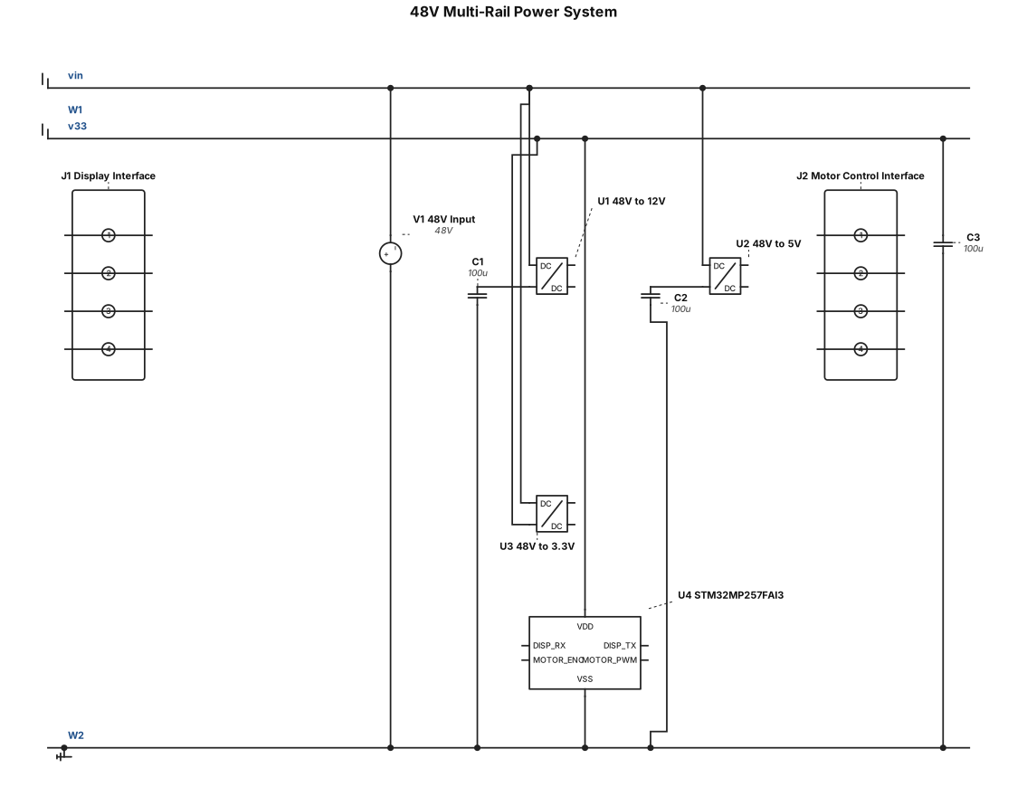
The system operates on a 48 V input, which is converted into 12 V, 5 V, and 3.3 V power rails. The 3.3 V rail supplies power to the STM32MP257FAI3 processor, which serves as the central controller and provides communication interfaces for the display and motor control systems.The system operates on a 48 V input, which is converted into 12 V, 5 V, and 3.3 V power rails. The 3.3 V rail supplies power to the STM32MP257FAI3 processor, which serves as the central controller and provides communication interfaces for the display and motor control systems.
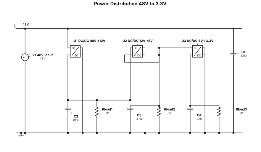
The system receives a 48 V input, which is converted through a DC/DC converter to the required low-voltage rails like 12 V, 5 V and 3.3 V rails. The proposed power hierarchy is therefore: 48 V Input → DC/DC Converter → 12 V → 5 V → 3.3 V The final voltage architecture should be confirmed based on the actual requirements of the MPU, communication transceivers, sensors, display and other loads.
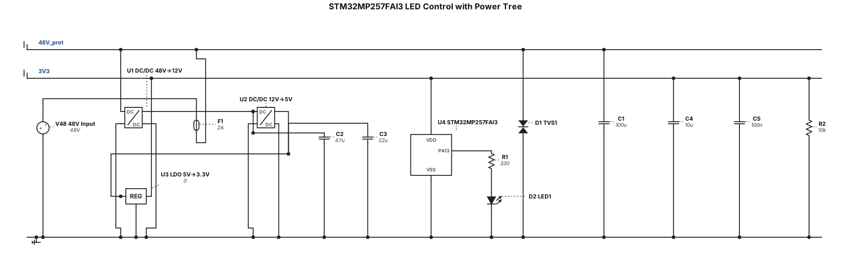
a circuit with STM32MP257FAI3 processor with actual pin outs and the input 3,3 V and it suppose to controller the LED on and Off. also put the over voltage protection as well. The system receives a 48 V input, which is converted through a DC/DC converter to the required low-voltage rails like 12 V, 5 V and 3.3 V rails. The proposed power hierarchy is therefore: 48 V Input → DC/DC Converter → 12 V → 5 V → 3.3 V The final voltage architecture should be confirmed based on the actual requirements of the MPU, communication transceivers, sensors, display and other loads.
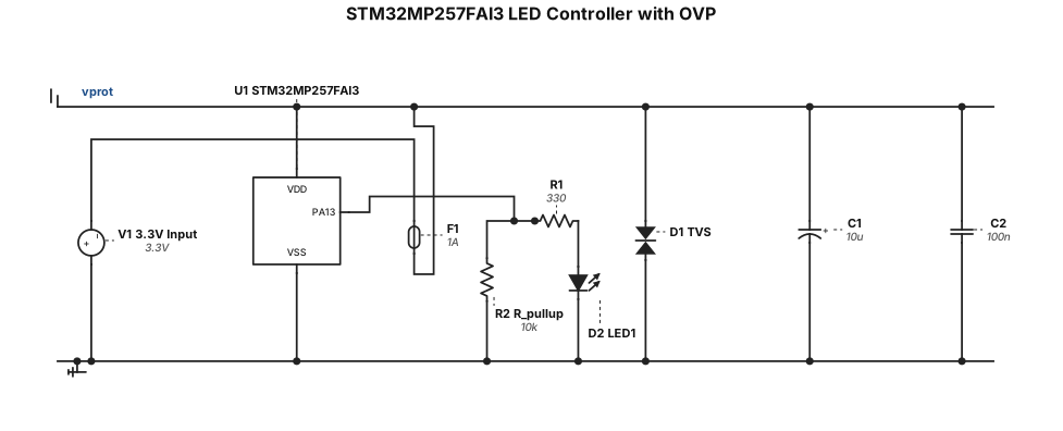
a circuit with STM32MP257FAI3 processor with actual pin outs and the input 3,3 V and it suppose to controller the LED on and Off. also put the over voltage protection as well.