
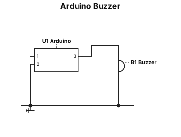
| Buzzer (+) to arduino Digital Pin 8 | | Buzzer (-) arduino Pin GND use my labels only
ENGINEERING DRAWING ARCHIVE · REAL SPECS
Engineering Diagram Examples from Real Specifications
Browse eligible circuit, ladder, single-line, P&ID, breadboard, timing, and logic drawings with their original prompts.
Browse 538 real creationsCOMMUNITY OUTPUTS · EXACT PROMPTS
Main engineering studio
Showing 25–48 of 379. No stock examples or system defaults. Choose a tool, study a real result, then reopen its prompt as your starting point.
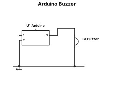
| Buzzer (+) to arduino Digital Pin 8 | | Buzzer (-) arduino Pin GND |
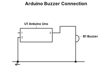
| Component | Arduino Pin | | ---------- | ------------- | | Buzzer (+) | Digital Pin 8 | | Buzzer (-) | GND |
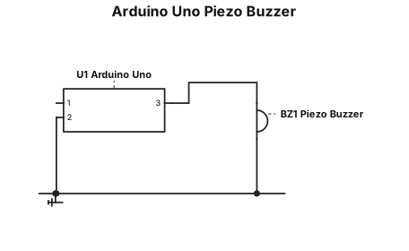
**Prompt for CircuitMaker AI:** Design a simple Arduino Uno piezo buzzer circuit using the following components: **1. Components** - Arduino Uno - Piezo Buzzer - Jumper Wires **2. Pin Mapping and Connections** | Component Pin | Arduino Pin | Connection | |---|---|---| | Buzzer (+) | Digital Pin 8 | Direct connection | | Buzzer (-) | GND | Direct connection | **3. Circuit Design Requirements** - Connect the positive terminal of the piezo buzzer to Arduino Digital Pin 8. - Connect the negative terminal of the piezo buzzer to Arduino GND. - Use appropriate jumper wires. - Clearly label all component names and pin connections. - Show the Arduino Uno and piezo buzzer in a clean, organized circuit layout. - Ensure the circuit is electrically correct and suitable for a beginner-level Arduino project. **4. Expected Output** Generate a clear circuit schematic showing all components, wiring connections, and Arduino pin labels.
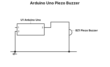
Elements/Components Arduino Uno Piezo Buzzer Jumper wires 4. Pin Mapping & Connections Component Pin Arduino Pin Wiring Connection Note Buzzer (+) Digital 8 Direct connection Buzzer (-) GND Direct connection
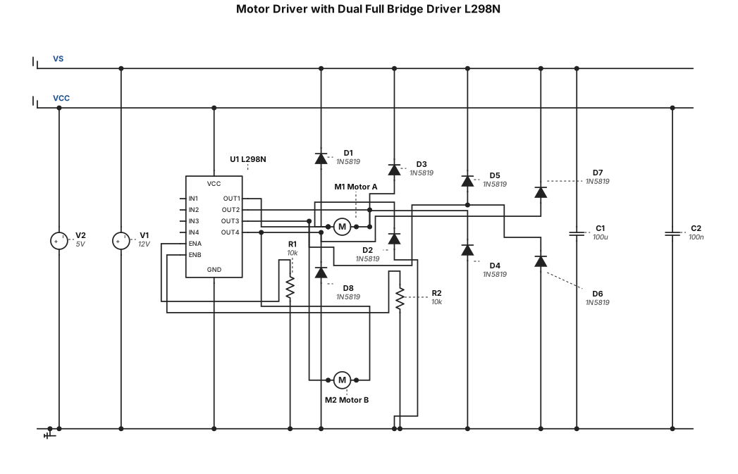
Motor driver withe dual full bridg driver l298n
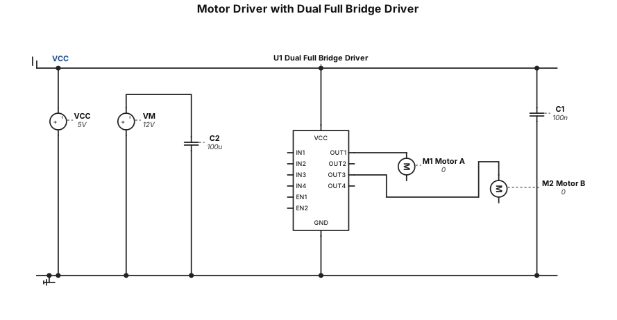
Motor driver withe dual full bridg driver
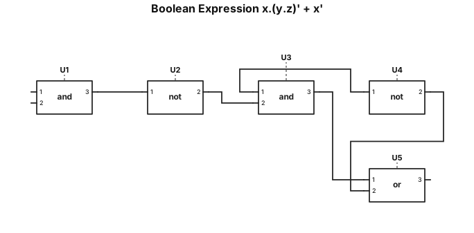
2. Draw circuits for the Boolean expressions outlined below. Complete the truth tables for these expressions and verify the truth tables using your circuits, x.¯("y.z" )+¯x
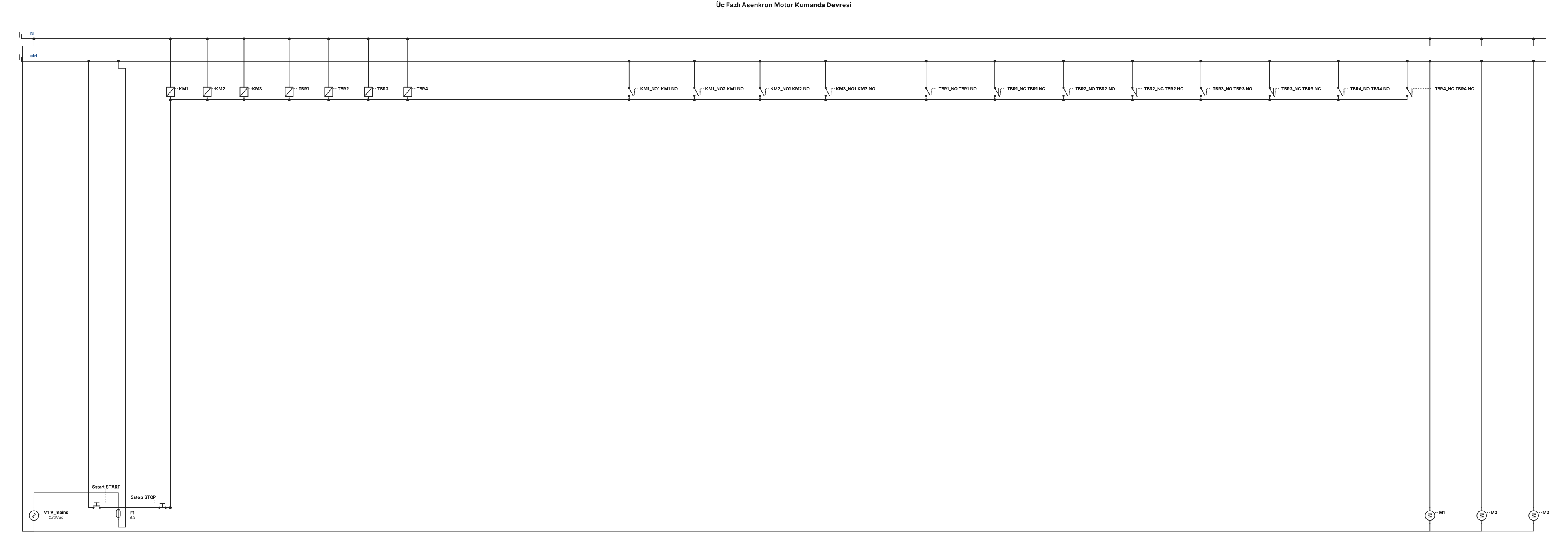
3 adet üç fazlı asenkron motor (M1, M2, M3), 4 adet düz zaman rölesi (TBR1, TBR2, TBR3, TBR4), 1 adet START ve 1 adet STOP butonu kullanarak klasik kontaktörlü kumanda devresi çiz. Çalışma sırası: 1. START butonuna basılınca M1 ve M2 aynı anda çalışmaya başlasın. TBR1 (4 saniye) devreye girsin. 2. TBR1’in 4 saniyelik süresi dolunca M2 dursun, M3 çalışmaya başlasın. TBR2 (4 saniye) devreye girsin. M1 çalışmaya devam etsin. 3. TBR2’nin 4 saniyelik süresi dolunca M3 dursun. M1 çalışmaya devam etsin. 4. STOP butonuna basılınca M1 dursun, M2 yeniden çalışmaya başlasın. TBR3 (6 saniye) devreye girsin. 5. TBR3’ün 6 saniyelik süresi dolunca M2 dursun, M3 çalışsın. TBR4 (4 saniye) devreye girsin. 6. TBR4’ün 4 saniyelik süresi dolunca M3 dursun ve bütün sistem tamamen kapansın. Devre çiziminde dikkat edilecekler: * PLC kullanılmasın. * Klasik röleli kumanda devresi çizilsin. * KM1, KM2 ve KM3 kontaktörleri kullanılsın. * Düz (çekmede gecikmeli) zaman rölelerinin NO ve NC kontakları kullanılsın. * Gerekli mühürleme ve yardımcı röle kontakları eklensin. * START ve STOP butonlarının görevleri doğru gösterilsin. * STOP butonu normal kapalı kontaklı olsun; durdurma sırasını başlatmak için gerekirse yardımcı kontağı kullanılsın. * Motorların çalışma sırası tam olarak verilen diyagrama uygun olsun. * Devre IEC standartlarına uygun, L ve N hatları arasında, anlaşılır bir merdiven tipi elektrik kumanda şeması olarak çizilsin. * Bütün kontaktör bobinleri, zaman rölesi bobinleri ve yardımcı kontaklar isimlendirilsin. * Devre tamamlandığında yeniden START verilene kadar sistem çalışmasın.
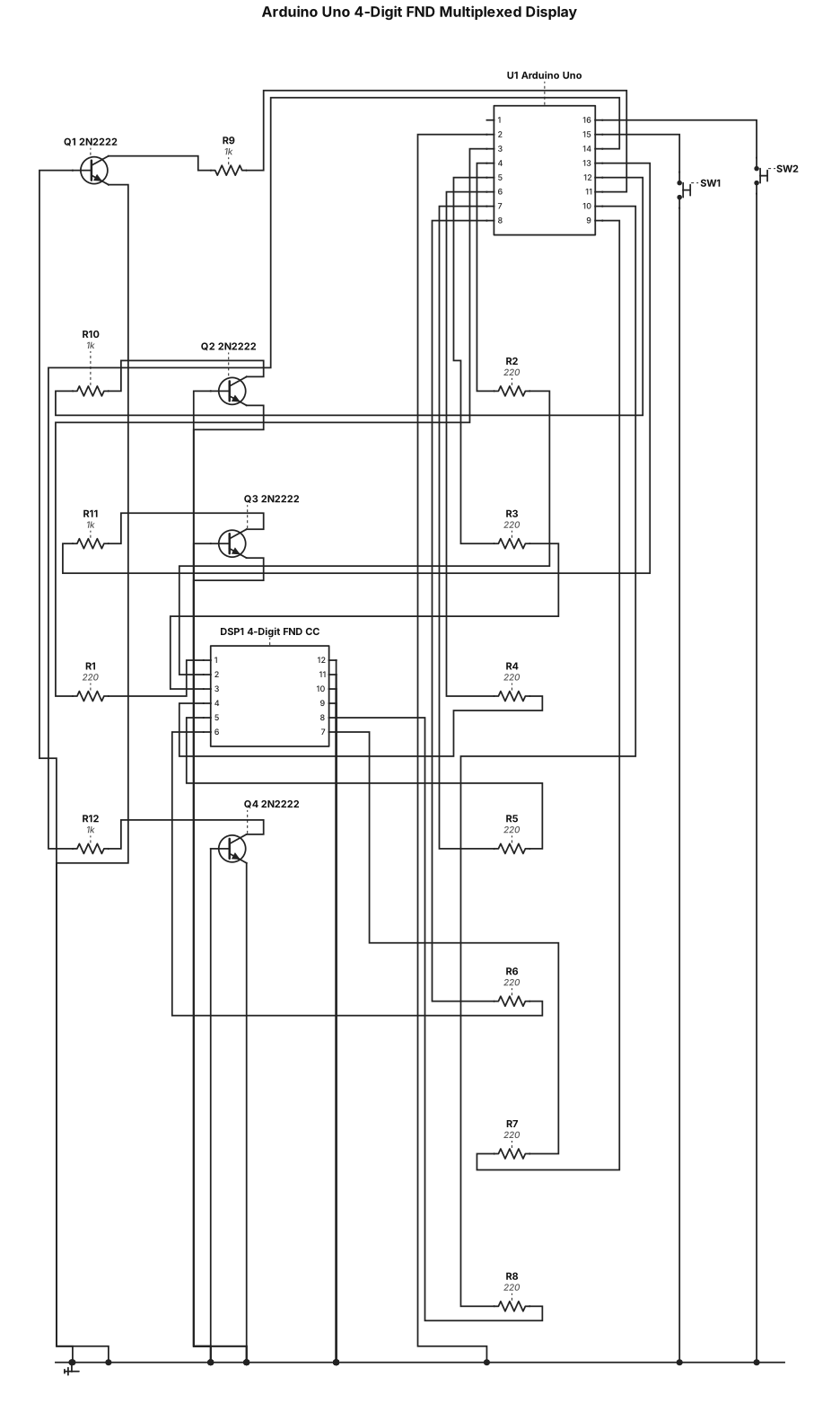
make a schematic on this Elements / Components Arduino Uno (or Mega) 4-Digit FND (Common Cathode) 4x NPN Transistors (e.g., 2N2222, BC547, or PMBT2222A) 8x 220Ω Resistors (for FND segments) 4x 1KΩ Resistors (for Transistor bases) 2x Push Buttons Jumper wires Breadboard 4. Pin Mapping & Connections Component Pin Arduino Pin Wiring Connection Note FND Pin 11 (A) Digital 2 Connect via 220Ω Resistor FND Pin 7 (B) Digital 3 Connect via 220Ω Resistor FND Pin 4 (C) Digital 4 Connect via 220Ω Resistor FND Pin 2 (D) Digital 5 Connect via 220Ω Resistor FND Pin 1 (E) Digital 6 Connect via 220Ω Resistor FND Pin 10 (F) Digital 7 Connect via 220Ω Resistor FND Pin 5 (G) Digital 8 Connect via 220Ω Resistor FND Pin 3 (DP) Digital 9 Connect via 220Ω Resistor FND Pin 12 (COM1) Digital 10 Connect to 1KΩ -> Transistor Base. Emitter to GND, Collector to COM1 FND Pin 9 (COM2) Digital 11 Connect to 1KΩ -> Transistor Base. Emitter to GND, Collector to COM2 FND Pin 8 (COM3) Digital 12 Connect to 1KΩ -> Transistor Base. Emitter to GND, Collector to COM3 FND Pin 6 (COM4) Digital 13 Connect to 1KΩ -> Transistor Base. Emitter to GND, Collector to COM4 SW1 (Leg 1) Analog A0 Connect one leg to A0, other leg to GND. (Internal Pull-up used) SW2 (Leg 1) Analog A1 Connect one leg to A1, other leg to GND. (Internal Pull-up used)
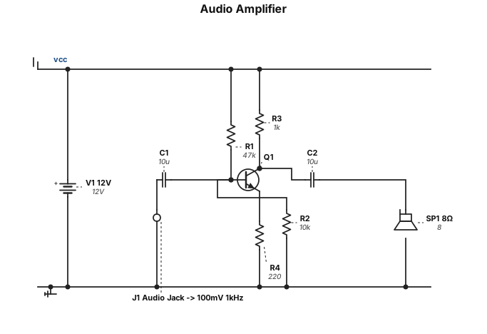
Create an EXACT REPLICA of the uploaded electronic circuit diagram. IMPORTANT: Treat the uploaded image as the absolute reference. Your task is to reproduce the same electronic schematic, NOT redesign it or create an alternative circuit. DO NOT CHANGE ANY COMPONENT, VALUE, CONNECTION, POSITION, OR CIRCUIT CONFIGURATION. ### 1. CIRCUIT COMPONENTS AND EXACT VALUES Include ONLY these components: 1. DC Power Supply: 12V battery 2. Transistor: Q1, NPN bipolar junction transistor 3. Resistor R1: 47kΩ 4. Resistor R2: 10kΩ 5. Resistor R3: 1kΩ 6. Resistor R4: 220Ω 7. Capacitor C1: 10µF 8. Capacitor C2: 10µF 9. Speaker: 8Ω 10. Audio input: Audio Jack, 100mV, 1kHz 11. Ground connection Do not add any other components. ### 2. EXACT CIRCUIT CONNECTIONS Follow the uploaded reference exactly. POWER SUPPLY: - Connect the positive terminal of the 12V battery to the upper power rail. - Connect the negative terminal to the bottom ground rail. TRANSISTOR BIAS NETWORK: - Connect the 47kΩ resistor between the positive power rail and the transistor base junction. - Connect the 10kΩ resistor between the transistor base junction and ground. - Connect the input 10µF capacitor between the audio input and transistor base junction. COLLECTOR NETWORK: - Connect the 1kΩ resistor between the positive power rail and transistor collector. - Connect the collector to the output 10µF capacitor. - The output capacitor must connect to the speaker branch. EMITTER NETWORK: - Connect the transistor emitter to the 220Ω resistor. - Connect the other end of the 220Ω resistor to ground. SPEAKER OUTPUT: - Connect the output 10µF capacitor in series with the 8Ω speaker. - Connect the other terminal of the speaker to ground. AUDIO INPUT: - Show the audio jack input on the left side. - Label it exactly: Audio Jack -> 100mV 1kHz. - Connect it through the input 10µF capacitor to the transistor base. ### 3. EXACT
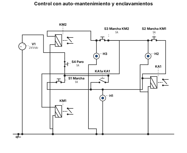
S1 activa KA1 y KA1 tiene auto-mantenimiento. S2 solo puede activar KM1 si KA1 está activado. S3 solo puede activar KM2 si KM1 está activado. S4 es un pulsador de paro NC que desactiva los tres elementos. H1, H2 y H3 se encienden respectivamente con KA1, KM1 y KM2.
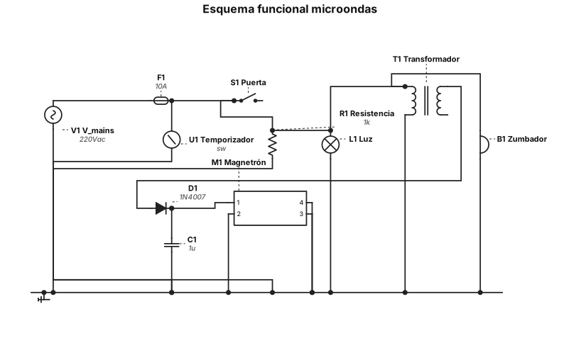
Esquema funcional microondas

Esquema funcional de: Tiene un baño de 4m2, un almacén de 6m2 y una sala médica de socorro y asistencia Tiene un pozo de 4m de profundidad del que sacar agua y un depósito a llenar de 1m3 subido a 5m de altura. Tiene una nevera de medicamentos, microondas, radio para comunicarse, 6 tomas de corriente, medidor de tensión y pulsaciones, luz de quirófano, máquina de oxígeno, calefacción por bomba de calor.
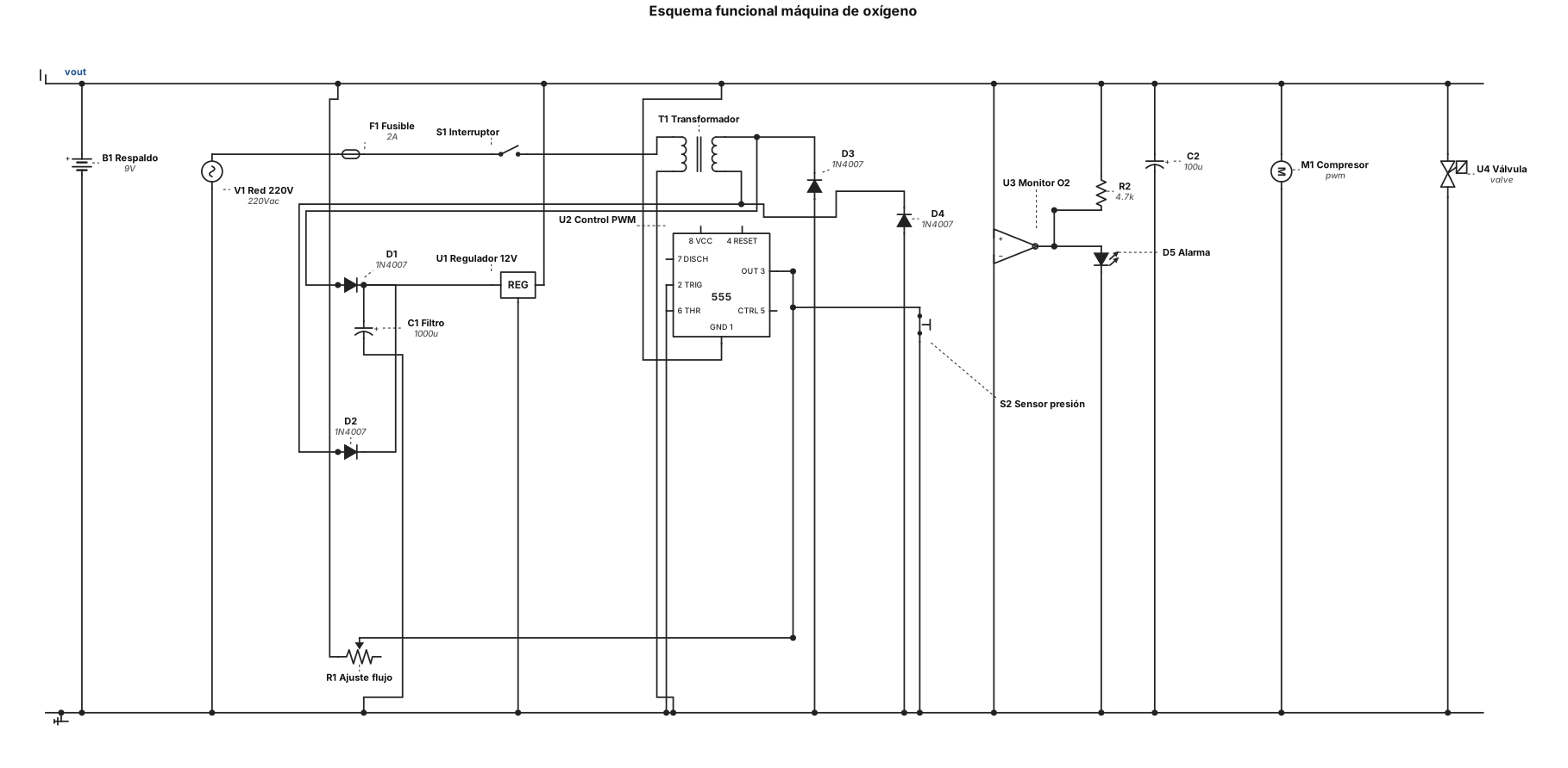
Esquema funcional maquina de oxigeno
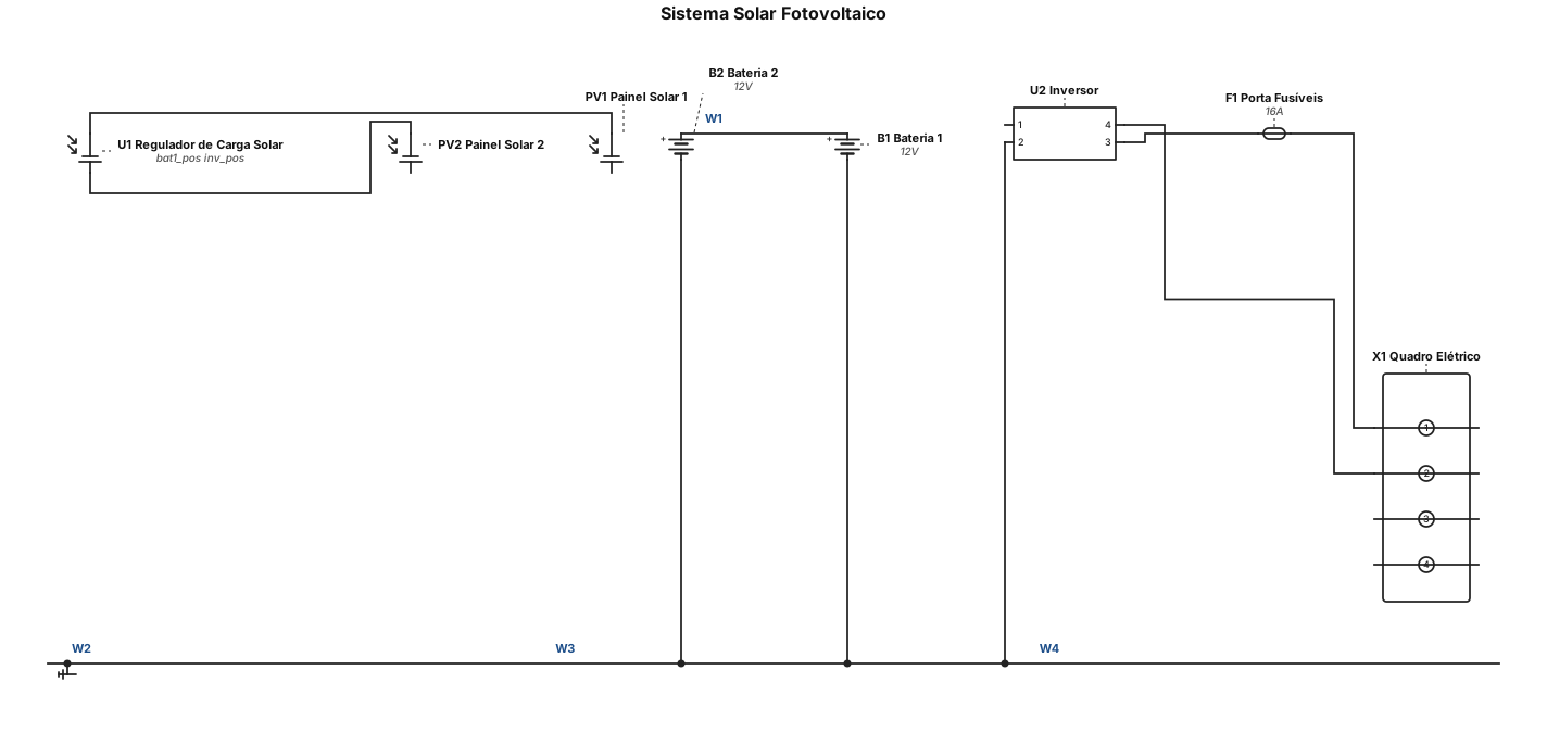
2 baterias, 2 painéis solares fotovoltaicos, 1 inversor, 1 regulador de carga solar, 1 quadro eletrico, 1 porta fusiveis
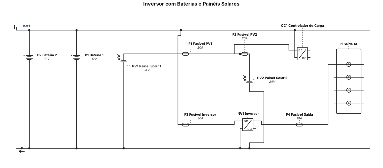
Inversor, 2 baterias, rolador de carga, dois painéis solares fotovoltaicos, porta fusiveis

Create a realistic, front-view electrical distribution panel layout for a 230V single-phase garden lighting system. Show one 2-pole main circuit breaker, one 2-pole 30mA RCD, and three 1-pole MCBs for three separate lighting circuits. Include DIN rails, neutral and protective earth terminal bars, and clearly labeled brown live, blue neutral, and green-yellow protective earth conductors. Show a conceptual layout with visible devices and wire routing, not just abstract circuit symbols. Do not assume the design is approved for installation.
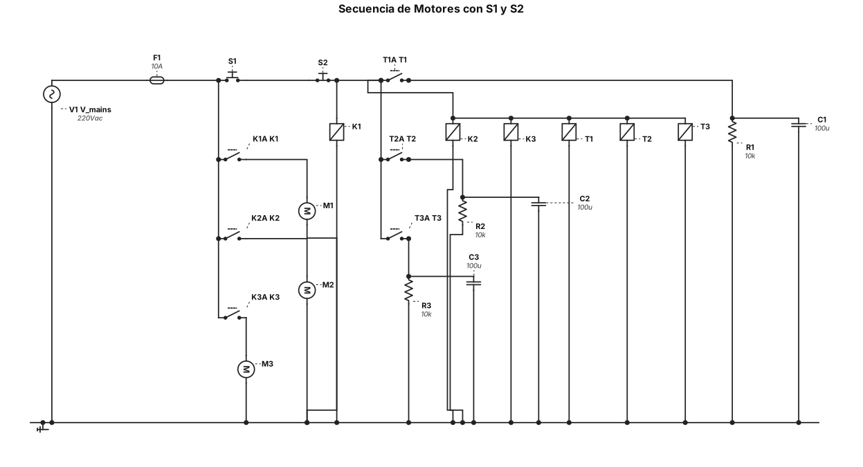
s1 enciende motor 1 3 seg enciende motor 2 vuelvo a presionar s1 y ahora enciende motor 3 en el apagado stop s2 S2 es para apagar, con s2 apago motor 3 , 3 segundos después apaga motor 2 y 3 segundos después apaga el motor 1, plano técnico completo en formato de imagen de alta resolución, con la misma estética profesional, simbología normalizada IEC 60617 / EN 81346 y disposición de CADe_SIMU 4.2 que mostraste en tu ejemplo
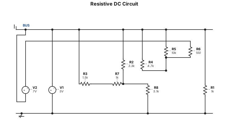
Draw a resistive DC circuit with 2 voltage sources and 8 resistors, with the following components and connections. COMPONENTS: - V1: 5 V DC voltage source (+ on top, - on bottom), placed on the left side, vertical. - V2: 7 V DC voltage source (+ on top, - on bottom), placed on the right side, vertical. - R1 = 1 kΩ - R2 = 3.3 kΩ - R3 = 1.5 kΩ - R4 = 4.7 kΩ - R5 = 10 kΩ - R6 = 100 Ω - R7 = 1 kΩ - R8 = 5.1 kΩ NODES (wires with the same name are the same electrical node): Node BUS (long horizontal wire in the middle of the circuit): - V1 positive terminal (+) - Top terminal of R1 - Bottom terminal of R5 - Top terminal of R2 - Top terminal of R3 - V2 negative terminal (-) - Left end of the wire that goes up to R4 (the left wire from the + side of V1 up to the left terminal of R4) Node TOP (upper middle node): - Right terminal of R4 - Top terminal of R5 - Left terminal of R6 Node VB1 (bottom left): - V1 negative terminal (-) - Bottom terminal of R1 - Left terminal of R8 Node VB2 (bottom middle): - Right terminal of R8 - Bottom terminal of R2 - Left terminal of R7 Node VB3 (bottom right): - Right terminal of R7 - Bottom terminal of R3 Node VX (upper right): - Right terminal of R6 - V2 positive terminal (+) LAYOUT (top to bottom): - Top row, left to right: R4 (4.7 kΩ) -> junction TOP -> R6 (100 Ω) -> V2 (7 V, vertical, on the right edge). - R5 (10 kΩ) hangs vertically from junction TOP down to the BUS wire. - Middle row: long horizontal BUS wire from the left edge to the right edge, with junction dots at the V1 terminal, at the R1 top, at the R5 bottom, at the R2 top and at the V2 bottom / R3 top. - Bottom area: V1 (5 V, vertical) on the left edge, R1 (1 kΩ), R2 (3.3 kΩ) and R3 (1.5 kΩ) hang vertically from the BUS wire. - Bottom row, left to right: wire from V1(-) to the bottom of R1, then R8 (5.1 kΩ) to the bottom of R2, then R7 (1 kΩ) to the bottom of R3. Use V1 negative terminal (node VB1) as ground (0 V). Draw it in a breadboard
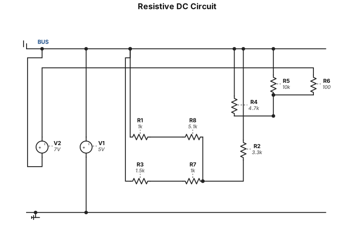
Draw a resistive DC circuit with 2 voltage sources and 8 resistors, with the following components and connections. COMPONENTS: - V1: 5 V DC voltage source (+ on top, - on bottom), placed on the left side, vertical. - V2: 7 V DC voltage source (+ on top, - on bottom), placed on the right side, vertical. - R1 = 1 kΩ - R2 = 3.3 kΩ - R3 = 1.5 kΩ - R4 = 4.7 kΩ - R5 = 10 kΩ - R6 = 100 Ω - R7 = 1 kΩ - R8 = 5.1 kΩ NODES (wires with the same name are the same electrical node): Node BUS (long horizontal wire in the middle of the circuit): - V1 positive terminal (+) - Top terminal of R1 - Bottom terminal of R5 - Top terminal of R2 - Top terminal of R3 - V2 negative terminal (-) - Left end of the wire that goes up to R4 (the left wire from the + side of V1 up to the left terminal of R4) Node TOP (upper middle node): - Right terminal of R4 - Top terminal of R5 - Left terminal of R6 Node VB1 (bottom left): - V1 negative terminal (-) - Bottom terminal of R1 - Left terminal of R8 Node VB2 (bottom middle): - Right terminal of R8 - Bottom terminal of R2 - Left terminal of R7 Node VB3 (bottom right): - Right terminal of R7 - Bottom terminal of R3 Node VX (upper right): - Right terminal of R6 - V2 positive terminal (+) LAYOUT (top to bottom): - Top row, left to right: R4 (4.7 kΩ) -> junction TOP -> R6 (100 Ω) -> V2 (7 V, vertical, on the right edge). - R5 (10 kΩ) hangs vertically from junction TOP down to the BUS wire. - Middle row: long horizontal BUS wire from the left edge to the right edge, with junction dots at the V1 terminal, at the R1 top, at the R5 bottom, at the R2 top and at the V2 bottom / R3 top. - Bottom area: V1 (5 V, vertical) on the left edge, R1 (1 kΩ), R2 (3.3 kΩ) and R3 (1.5 kΩ) hang vertically from the BUS wire. - Bottom row, left to right: wire from V1(-) to the bottom of R1, then R8 (5.1 kΩ) to the bottom of R2, then R7 (1 kΩ) to the bottom of R3. Use V1 negative terminal (node VB1) as ground (0 V).
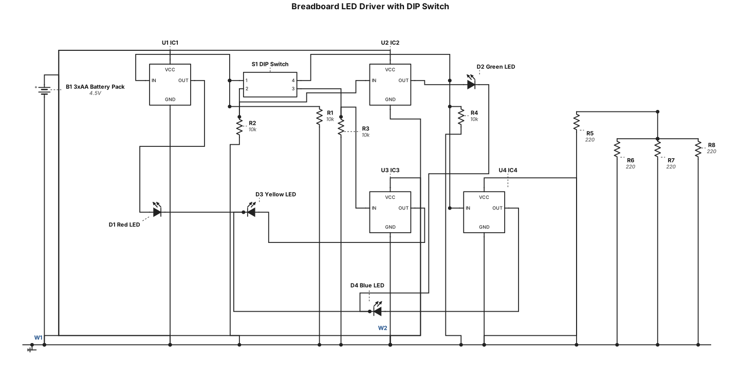
Generate a clean, top-down, 3D-rendered breadboard diagram in the style of Fritzing. White background. Components: 1 large breadboard (bottom) and 1 small breadboard (top). 1 battery pack (3 AA batteries) on the far left. 1 red 4-pin DIP switch on the bottom-left. 4 black IC chips (14-pin) stacked vertically in the middle of the large breadboard. 4 LEDs (Red, Green, Yellow, Blue) in a vertical row on the far right. Tan resistors (220 ohm) next to the LEDs. Tan resistors (10k ohm) next to the DIP switch. Wiring Instructions (Strictly follow these): Power: Red wires connect the battery (+) to the top and bottom Red rails. Black wires connect the battery (-) to the top and bottom Blue rails. Short red wires go from the Red rail to Pin 14 of all 4 chips. Short black wires go from the Blue rail to Pin 7 of all 4 chips. Inputs (Green Wires): Wires run from the DIP switch horizontally to the left-side input pins of all 4 chips. 10k resistors connect from the switch inputs to the Blue (-) rail. Outputs (Colored Wires): Orange, purple, white, and grey wires run from the output pins on the right side of the chips directly to the long legs of the 4 LEDs. LED Grounds: 220-ohm resistors connect the short legs of the LEDs to the bottom Blue (-) rail. Critical Rules: Do NOT route wires under the chips. Do NOT connect red wires to blue rails. The wiring must look physically possible, neat, and flat against the breadboard.
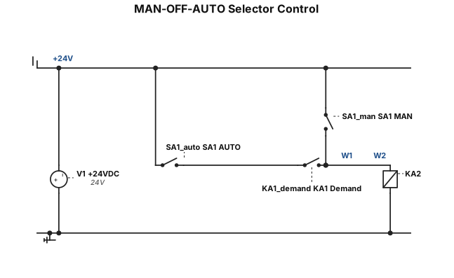
Generate an industrial IEC electrical control schematic, not a block diagram. Use 24 VDC ladder-style wiring with positive and negative rails. A three-position MAN-OFF-AUTO selector SA1 controls relay coil KA2. In MAN, a normally open SA1 manual contact directly energizes KA2. In AUTO, a normally open SA1 automatic contact in series with a normally open KA1 demand contact energizes KA2. OFF opens both branches. Draw the MAN and AUTO branches in parallel, joining before KA2. Label all components and show actual electrical connections.
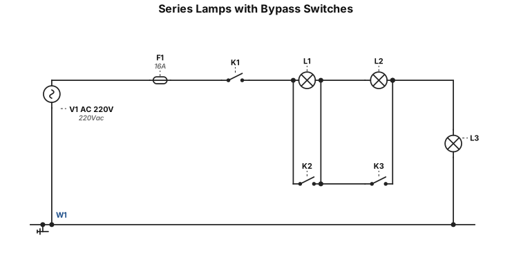
Create a clean horizontal schematic: - Left side: AC source 220V → Fuse F1 → Switch K1 - After K1, three lamps in a straight horizontal series line: L1 then L2 then L3 - Directly under L1, place switch K2 connected in parallel with L1 only - Directly under L2, place switch K3 connected in parallel with L2 only - L3 has no parallel switch - Right side of L3 connects down to the Neutral line - Neutral is a straight horizontal line at the bottom connecting back to the source Important: - All three lamps (L1, L2, L3) must be on the same horizontal line - Do not drop L3 down - K2 only bypasses L1 - K3 only bypasses L2 - Keep the diagram simple and classic like a textbook series circuit with two individual bypass switches