
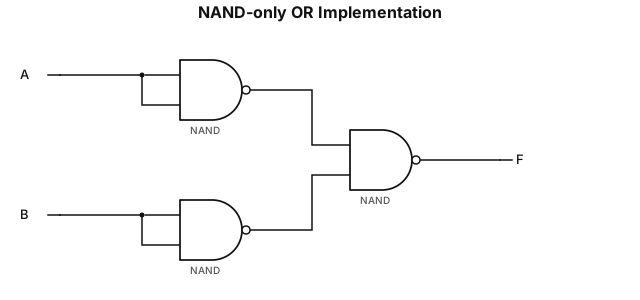
A logic gate diagram using only NAND gates to implement an OR operation, as shown in image_7.png. It features three NAND gates[cite: 3]. Inputs A and B are split: A is split and connected to both input pins of the top NAND gate (acting as an inverter for A'); B is split and connected to both input pins of the bottom-left NAND gate (acting as an inverter for B')[cite: 3]. The outputs of these two inverting NAND gates are then connected as inputs to a third, final 2-input NAND gate. Below the complete logic diagram, the text label is provided: "F=A+B=((A+B)')'=((AA)' (BB)')'" [cite: 3, 4]. All gate outlines are in the light blue color as seen in image_7.png.
ENGINEERING DRAWING ARCHIVE · REAL SPECS
Engineering Diagram Examples from Real Specifications
Browse eligible circuit, ladder, single-line, P&ID, breadboard, timing, and logic drawings with their original prompts.
Browse 540 real creationsCOMMUNITY OUTPUTS · EXACT PROMPTS
All visitor creations
Showing 169–192 of 540. No stock examples or system defaults. Choose a tool, study a real result, then reopen its prompt as your starting point.
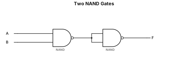
A logic gate diagram showing two NAND gates[cite: 3]. The first NAND gate has two inputs, labeled A and B. The output of the first NAND gate connects to a single dot, which then splits and connects to both input ports of the second NAND gate[cite: 3]. The final output from the second NAND gate should be labeled with the text "F=AB=((AB)')'".
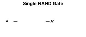
A logic gate diagram showing a single NAND gate[cite: 3]. Input A splits into two branches and connects to both input pins of the NAND gate[cite: 3]. The output pin of the NAND gate is labeled as A'[cite: 3].
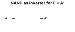
A logic gate diagram for F = A' using a 2-input NAND gate configured as an inverter. Input A is split into both inputs of the NAND gate, and the final output terminal is labeled as A'.
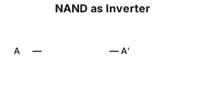
A logic gate diagram for A' using a 2-input NAND gate configured as an inverter (NOT gate). Single input A is split and connected to both inputs of the NAND gate, and the output is ( A').
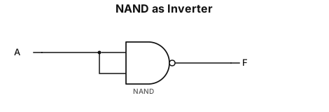
A logic gate diagram for F = A' using a 2-input NAND gate configured as an inverter (NOT gate). Single input A is split and connected to both inputs of the NAND gate, and the output is ( A').
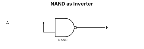
A logic gate diagram for F = A' using a 2-input NAND gate configured as an inverter (NOT gate). Single input A is split and connected to both inputs of the NAND gate, and the output is F (or A').
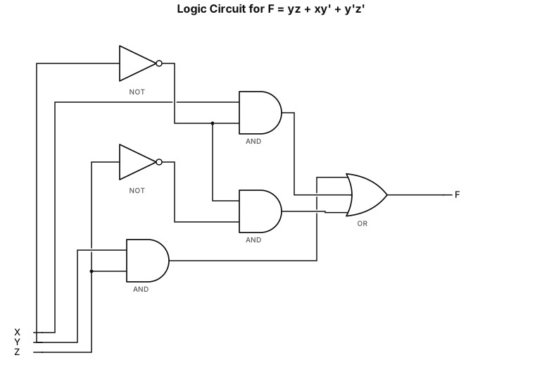
A logic gate circuit for F = yz + xy' + y'z' with inputs X, Y, Z and output F. It uses two NOT gates for Y' and Z', three AND gates for terms (y and z), (x and y'), and (y' and z'), and one 3-input OR gate connecting all AND gate outputs to F.
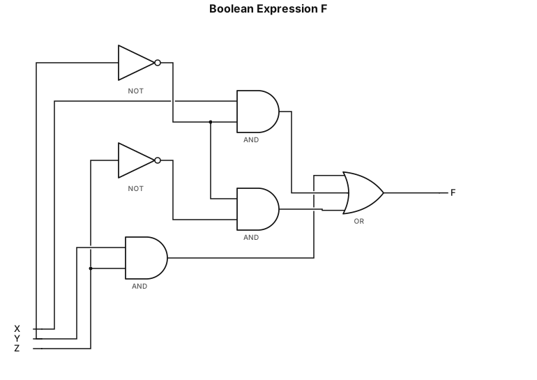
Create a logic gate diagram for the Boolean expression: F = (Y AND Z) OR (X AND NOT Y) OR (NOT Y AND NOT Z). Use exactly: 3 AND gates with 2 inputs each. 2 NOT gates (one for Y and one for Z). 1 OR gate with 3 inputs. Arrange the gates vertically, just like a standard sum-of-products circuit: Top AND gate: inputs Y and Z. Middle AND gate: inputs X and NOT Y. Bottom AND gate: inputs NOT Y and NOT Z. Connect all three AND gate outputs to a single 3-input OR gate on the right. Show input labels X, Y, Z on the left and output F on the right. Use clear wires, junction dots, and standard logic gate symbols. Do not simplify the Boolean expression. Keep the layout clean and similar to a textbook logic circuit diagram.
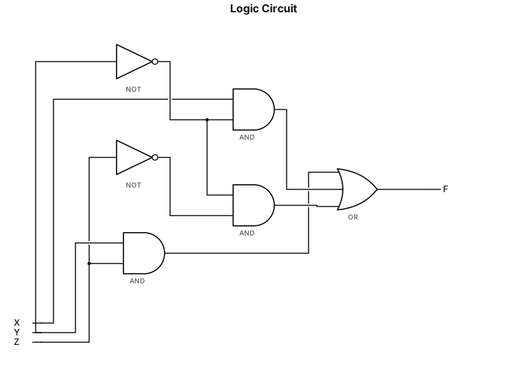
verilog module logic_circuit( input X, Y, Z, output F ); wire Y_n; wire Z_n; wire A, B, C; not (Y_n, Y); not (Z_n, Z); and (A, Y, Z); and (B, X, Y_n); and (C, Y_n, Z_n); or (F, A, B, C); endmodule
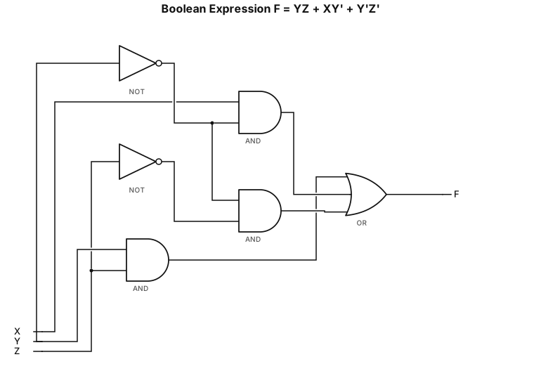
Create a digital logic circuit for this exact Boolean expression: F = YZ + XY' + Y'Z' GATE REQUIREMENTS: 3 two-input AND gates 2 NOT gates 1 three-input OR gate CONNECTIONS: AND1 = Y AND Z AND2 = X AND NOT(Y) AND3 = NOT(Y) AND NOT(Z) Connect the three AND gate outputs to one 3-input OR gate. The OR gate output must be labeled F. LAYOUT: Place inputs X, Y, Z on the left. Place NOT gates on the Y and Z input branches. Arrange three AND gates vertically in the center. Place one OR gate on the right. Connect all wires exactly according to the Boolean expression. Use standard digital logic symbols. Use black wires, black junction dots and blue gate outlines. White background. Keep the circuit clean and symmetrical. Do not change or simplify the Boolean expression. Do not add unnecessary gates.
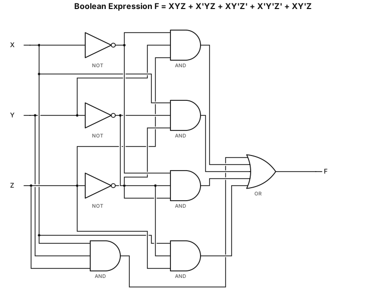
Draw an exact digital logic circuit for the following Boolean expression: F = XYZ + X'YZ + XY'Z' + X'Y'Z' + XY'Z Circuit requirements: Three NOT gates to generate X', Y', and Z'. Five 3-input AND gates: AND1 = X AND Y AND Z AND2 = NOT(X) AND Y AND Z AND3 = X AND NOT(Y) AND NOT(Z) AND4 = NOT(X) AND NOT(Y) AND NOT(Z) AND5 = X AND NOT(Y) AND Z One 5-input OR gate. Connect all five AND gate outputs to the five OR gate inputs. Label inputs X, Y, Z and output F. Layout: Inputs on the left. Five AND gates vertically aligned in the center. NOT gates positioned on the input branches. One OR gate on the right. Black wires and black junction dots. Blue logic gate outlines. White background. Use standard digital logic symbols. Arrange the circuit like the provided reference image. Do not simplify the Boolean expression. Do not omit any gate or input connection.
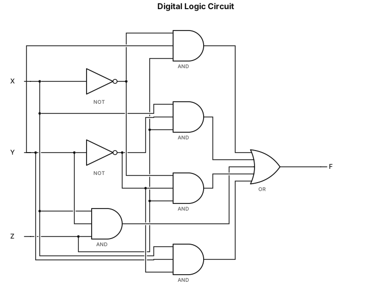
Create a digital logic circuit diagram. INPUTS: X, Y, Z LOGIC GATES: - 5 AND gates - 2 NOT gates - 1 OR gate LAYOUT: - Place X, Y, Z input lines on the left. - Place 5 AND gates vertically in the center. - Place 2 NOT gates before the corresponding AND gate inputs. - Connect all 5 AND gate outputs to one OR gate. - Place the OR gate on the right. - Label the final output as F. DESIGN: - Use standard digital logic gate symbols. - Black straight connecting wires. - Blue AND, OR and NOT gate outlines. - Black junction dots. - Keep the same arrangement as the reference image. - White background. - Export as SVG or PNG.
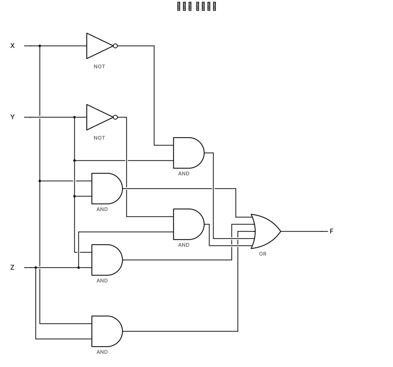
입력 X, Y, Z를 사용하는 디지털 논리회로를 그려줘. AND 게이트 5개와 NOT 게이트 2개를 사용하고, 각 게이트의 출력을 마지막 OR 게이트에 연결해줘. 입력은 왼쪽에 X, Y, Z로 표시하고 출력은 오른쪽에 F로 표시해줘. 검은색 직선 배선과 표준 논리회로 기호를 사용하고, 첨부한 회로도와 비슷한 형태로 깔끔하게 배치해줘.
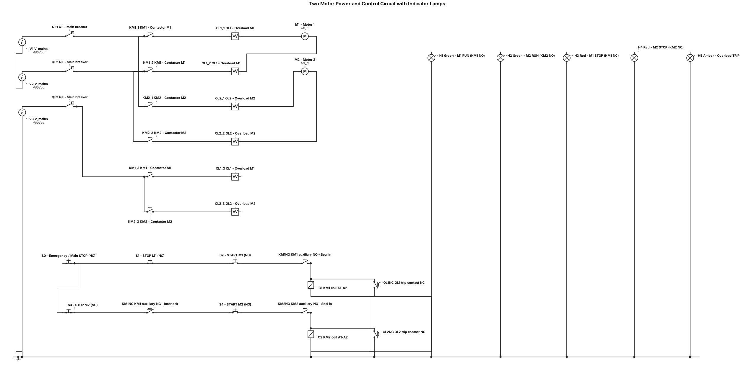
digraph MotorControl { graph [rankdir=TB, splines=ortho, nodesep=0.4, ranksep=0.6, label="TWO MOTOR POWER AND CONTROL CIRCUIT WITH INDICATOR LAMPS", labelloc=t]; node [shape=box, style="rounded", fontname="Arial"]; subgraph cluster_power { label="POWER CIRCUIT - 3 PHASE"; L1; L2; L3; QF [label="QF - Main breaker"]; KM1 [label="KM1 - Contactor M1"]; OL1 [label="OL1 - Overload M1"]; M1 [label="M1 - Motor 1"]; KM2 [label="KM2 - Contactor M2"]; OL2 [label="OL2 - Overload M2"]; M2 [label="M2 - Motor 2"]; L1 -> QF; L2 -> QF; L3 -> QF; QF -> KM1 -> OL1 -> M1; QF -> KM2 -> OL2 -> M2; } subgraph cluster_control { label="CONTROL CIRCUIT - LADDER"; S0 [label="S0 - Emergency / Main STOP (NC)"]; S1 [label="S1 - STOP M1 (NC)"]; S2 [label="S2 - START M1 (NO)"]; KM1NO [label="KM1 auxiliary NO - Seal in"]; C1 [label="KM1 coil A1-A2"]; S3 [label="S3 - STOP M2 (NC)"]; S4 [label="S4 - START M2 (NO)"]; KM1NC [label="KM1 auxiliary NC - Interlock"]; KM2NO [label="KM2 auxiliary NO - Seal in"]; C2 [label="KM2 coil A1-A2"]; OL1NC [label="OL1 trip contact NC"]; OL2NC [label="OL2 trip contact NC"]; S0 -> S1 -> S2 -> C1; S2 -> KM1NO -> C1; S0 -> S3 -> KM1NC -> S4 -> C2; S4 -> KM2NO -> C2; OL1NC -> C1; OL2NC -> C2; } subgraph cluster_lamps { label="INDICATOR LAMPS"; H1 [label="H1 Green - M1 RUN (KM1 NO)"]; H2 [label="H2 Green - M2 RUN (KM2 NO)"]; H3 [label="H3 Red - M1 STOP (KM1 NC)"]; H4 [label="H4 Red - M2 STOP (KM2 NC)"]; H5 [label="H5 Amber - Overload TRIP"]; } }
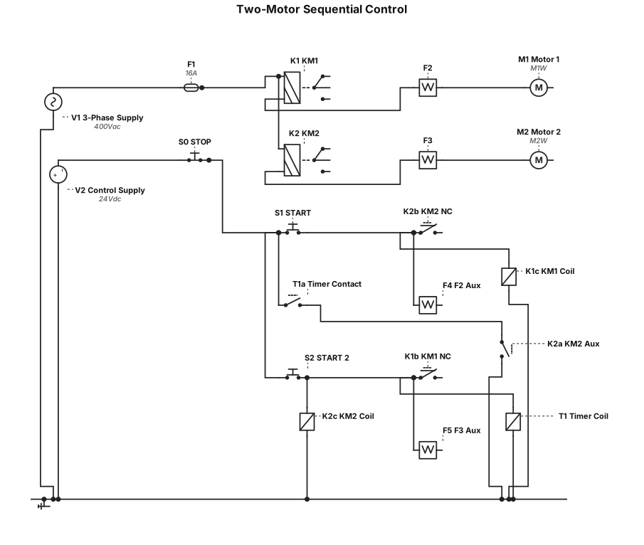
Design the power and control circuits for two three-phase asynchronous motors operating under the following conditions: When the START push button is pressed, only Motor 1 will start. Motor 1 will stop when the STOP push button or the START 2 push button is pressed. When the STOP push button is pressed, Motor 1 will stop and Motor 2 will start. Motor 2 will stop automatically after running for 10 seconds. The system will be protected by thermal overload relays. The two motors must never operate simultaneously. Design the required control and power circuits using standard IEC electrical symbols. Draw the power and control circuits separately, label all components, and show all wiring connections clearly.
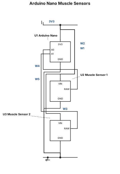
Draw three rectangular circuit blocks labeled Arduino Nano, Muscle Sensor 1, and Muscle Sensor 2. The Arduino Nano block has terminals labeled 3V3, GND, A0, and A1. Each muscle sensor block has terminals labeled VIN, GND, and RAW. Connect 3V3 to both VIN terminals. Connect Arduino GND to both sensor GND terminals. Connect Sensor 1 RAW to A0. Connect Sensor 2 RAW to A1. Show a connection dot at each branching junction.
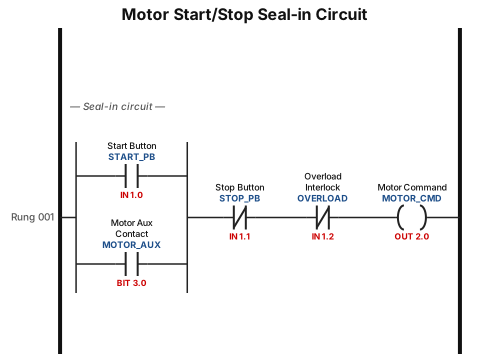
A motor start-stop seal-in ladder circuit with a normally closed stop button, normally open start button, motor auxiliary contact, overload interlock, and motor command coil.
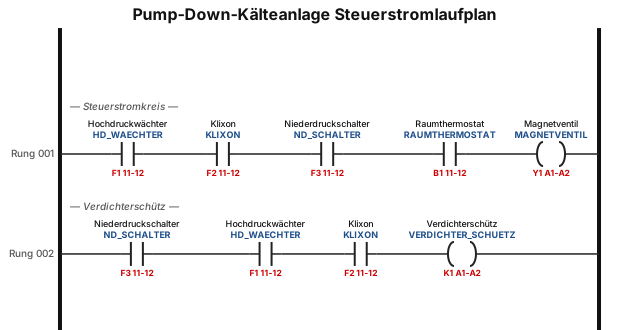
Erstelle einen Steuerstromlaufplan einer Pump-Down-Kälteanlage. L1 oben, N unten, senkrechte Strompfade. Mit Hochdruckwächter, Klixon, Niederdruckschalter, Verdichterschütz und Raumthermostat mit Magnetventil. Verwende IEC-Schaltzeichen und Anschlussnummern.
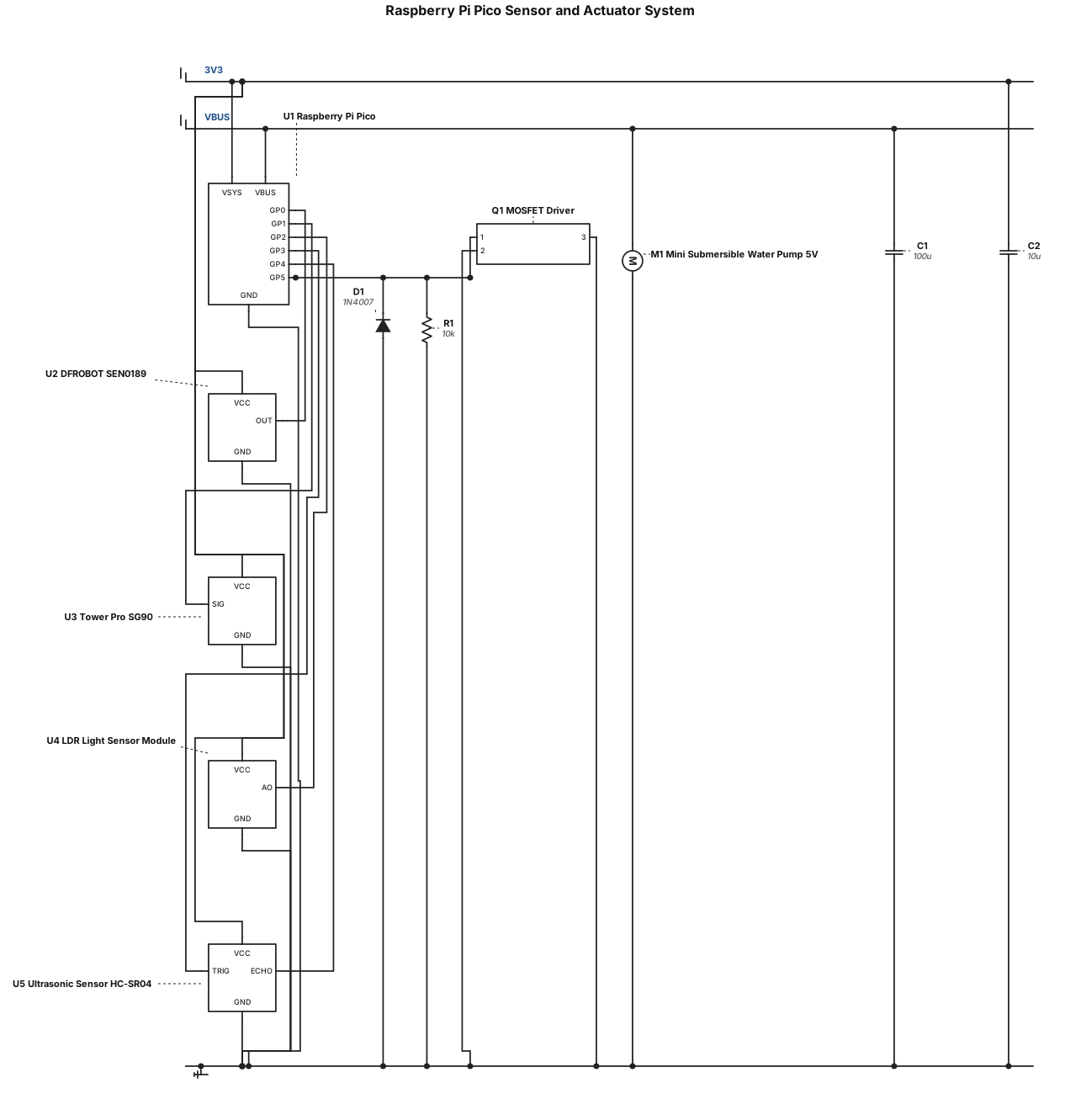
A raspberry Pi Pico connected to a DFROBOT SEN0189, Tower Pro SG90, LDR Light Sensor Module, Ultrasonic Sensor, and Mini Submersible Water Pump (5 Volts). Use a breadboard for any extra connections.
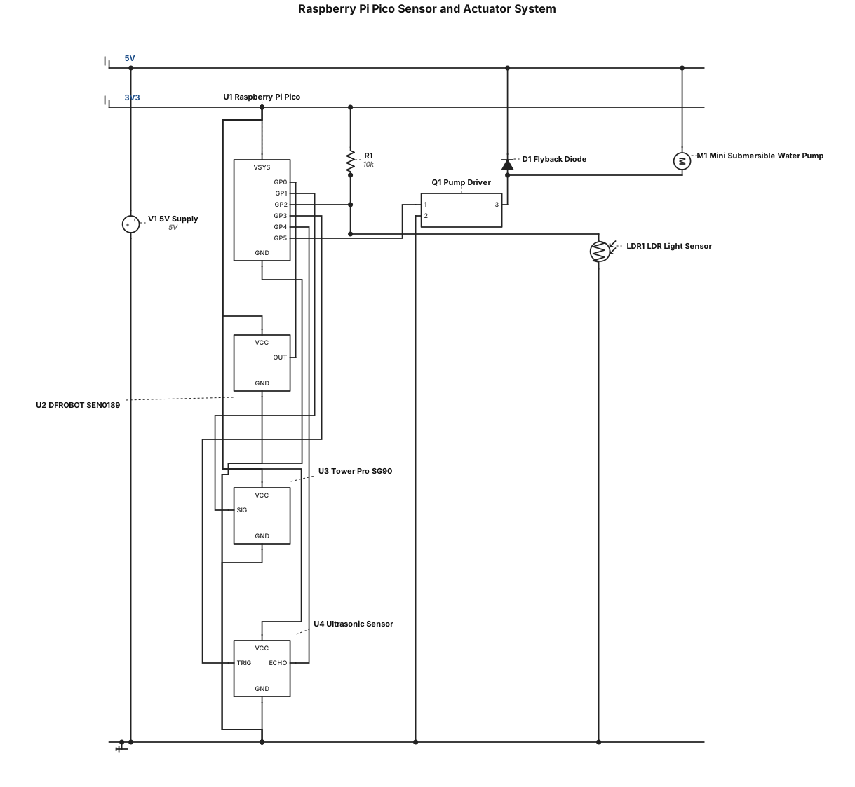
A raspberry Pi Pico connected to a DFROBOT SEN0189, Tower Pro SG90, LDR Light Sensor Module, Ultrasonic Sensor, and Mini Submersible Water Pump (5 Volts)
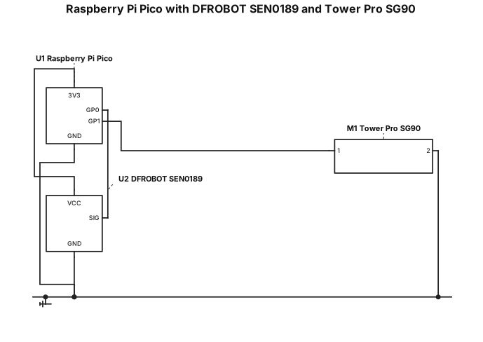
A raspberry Pi Pico connected to a DFROBOT SEN0189 and Tower Pro SG90
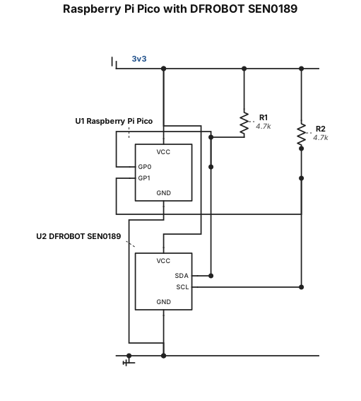
A raspberry Pi Pico connected to a DFROBOT SEN0189
%3B%20B%20is%20split%20and%20connected%20to%20both%20input%20pins%20of%20the%20bottom-left%20NAND%20gate%20(acting%20as%20an%20inverter%20for%20B')%5Bcite%3A%203%5D.%20The%20outputs%20of%20these%20two%20inverting%20NAND%20gates%20are%20then%20connected%20as%20inputs%20to%20a%20third%2C%20final%202-input%20NAND%20gate.%20Below%20the%20complete%20logic%20diagram%2C%20the%20text%20label%20is%20provided%3A%20%22F%3DA%2BB%3D((A%2BB)')'%3D((AA)'%20(BB)')'%22%20%5Bcite%3A%203%2C%204%5D.%20All%20gate%20outlines%20are%20in%20the%20light%20blue%20color%20as%20seen%20in%20image_7.png.)
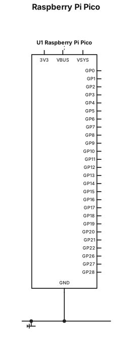
A raspberry Pi Pico